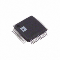
AD9763ASTZ Analog Devices Inc, AD9763ASTZ Datasheet - Page 23

AD9763ASTZ
Manufacturer Part Number
AD9763ASTZ
Description
IC DAC 10BIT DUAL 125MSPS 48LQFP
Manufacturer
Analog Devices Inc
Series
TxDAC+®r
Specifications of AD9763ASTZ
Data Interface
Parallel
Settling Time
35ns
Number Of Bits
10
Number Of Converters
2
Voltage Supply Source
Analog and Digital
Power Dissipation (max)
450mW
Operating Temperature
-40°C ~ 85°C
Mounting Type
Surface Mount
Package / Case
48-LQFP
Resolution (bits)
10bit
Sampling Rate
125MSPS
Input Channel Type
Parallel
Supply Voltage Range - Analog
3V To 5.5V
Supply Voltage Range - Digital
2.7V To 5.5V
Lead Free Status / RoHS Status
Lead free / RoHS Compliant
For Use With
AD9763-EBZ - BOARD EVAL FOR AD9763
Lead Free Status / RoHS Status
Lead free / RoHS Compliant, Lead free / RoHS Compliant
Available stocks
Company
Part Number
Manufacturer
Quantity
Price
Company:
Part Number:
AD9763ASTZ
Manufacturer:
ADI
Quantity:
180
Company:
Part Number:
AD9763ASTZ
Manufacturer:
Analog Devices Inc
Quantity:
10 000
Part Number:
AD9763ASTZ
Manufacturer:
ADI/亚德诺
Quantity:
20 000
Company:
Part Number:
AD9763ASTZRL
Manufacturer:
Analog Devices Inc
Quantity:
10 000
Part Number:
AD9763ASTZRL
Manufacturer:
ADI/亚德诺
Quantity:
20 000
EVALUATION BOARD
GENERAL DESCRIPTION
The AD9763-EB is an evaluation board for the AD9763 10-bit
dual digital-to-analog converter. Careful attention to layout and
circuit design, combined with a prototyping area, allow the user
to easily and effectively evaluate the AD9763 in any application
where high resolution, high speed conversion is required.
This board allows the user the flexibility to operate the AD9763
in various configurations. Possible output configurations
W R T 1 I N
W R T 2 I N
C L K 1 I N
C L K 2 I N
RC O M
RC O M
IQ W R T
R ESET
D V DD I N
IQ C L K
IQ SEL
S L EEP
BAN - J AC K
BAN - J AC K
1
1
S1
S2
S3
S4
I N P 2 3
I N P1
B 1
B 2
2
2
R 1
22 ?
R 1
22 ?
D G ND ; 3 , 4 , 5
D G ND ; 3 , 4 , 5
D G ND ; 3 , 4 , 5
D G ND ; 3 , 4 , 5
T P 1 0
R ED
I N P 2 4
I N P2
W H T
T P 3 3
3
3
W H T
T P 2 9
W H T
T P 3 0
W H T
T P 3 1
W H T
T P 3 2
B E A D
R 2
22 ?
R 2
22 ?
L 1
I N P 2 5
I N P3
4
4
1
2
R 3
22?
R 3
22?
R 1 3
50 ?
1
2
I N P 26
I N P4
C 9
10 µF
25 V
1
2
R 1
50 ?
5
5
R 4
22 ?
R 4
22 ?
I N P 2 7
I N P5
T P 3 7
B L K
1
2
6
6
R 2
50 ?
R 5
22 ?
R 5
22 ?
Figure 45. Power Decoupling and Clocks on AD9763 Evaluation Board
T P 4 3
B L K
I N P 2 8
I N P6
T P 3 8
D V D D
B L K
1
2
7
7
R 6
22 ?
R 6
22 ?
R 3
50 ?
I N P 2 9
I N P7
DC L KIN1
D G ND
T P 39
B L K
1
2
8
8
R7
22?
R7
22?
R4
50?
1
1
1
INP30
INP8
A
A
A
JP16
I
I
I
JP5
JP4
JP3
9
9
2
R8
22?
R8
22?
2
2
C
C
C
B
B
B
1
AVDDIN
3
3
3
A B
JP9
10
10
R9
22?
R9
22?
Rev. D | Page 23 of 32
2
RP16
RP10
BAN-JACK
BAN-JACK
3
B3
B4
TP11
DCLKIN2
RED
DVDD
RCOM
RCOM
BEAD
JP2
JP1
L2
include transformer coupled, resistor terminated, and single and
differential outputs. The digital inputs can be used in dual port
or interleaved mode, and are designed to be driven from various
word generators, with the on-board option to add a resistor
network for proper load termination. When operating the
AD9763, best performance is obtained when running the digital
supply (DVDD) at 3.3 V and the analog supply (AVDD) at 5 V.
DVDD
DVDD
1
1
/2 CLOCK DIVIDER
INP31
INP9
3
1
2
1
2
2
2
R1
22?
R1
22?
C10
10µF
25V
1
J
CLK
K
1
15
INP10
INP32
A B
A B
JP6
PRE
CLR
JP7
U1
2
2
3
3
4
DGND; 8
DVDD; 16
R2
22?
R2
22?
TP40
BLK
Q
Q
INP11
INP33
3
3
TP44
BLK
5
6
4
4
R3
22?
R3
22?
TSSOP11 2
TP41
AVDD
BLK
INP12
INP34
5
5
R4
22?
R4
22?
AG N D
TP 4 2
BL K
W R T 1
C L K 1
C L K 2
W R T 2
S L EEP
IN P 1 3
IN P 3 5
6
6
R 5
22 ?
R 5
22 ?
I N P 1 4
I N P 3 6
1 1
1 3
1 2
7
7
R 6
22 ?
R 6
22 ?
D V D D
J
C L K
K
1
2
1 0
1 4
P R E
C L R
C 7
0 . 1 µ F
U 2
8
8
R 7
22 ?
R 7
22 ?
D G ND; 8
D V DD; 16
I NCK1
I NCK2
Q
Q
9
9
R8
22?
R8
22?
9
7
1
2
TSSOP112
C8
0.01µF
10
10
R9
22?
R9
22?
RP15
RP9
AD9763
00617-045


