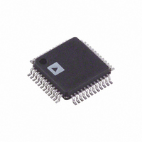
AD9763ASTZ Analog Devices Inc, AD9763ASTZ Datasheet - Page 17

AD9763ASTZ
Manufacturer Part Number
AD9763ASTZ
Description
IC DAC 10BIT DUAL 125MSPS 48LQFP
Manufacturer
Analog Devices Inc
Series
TxDAC+®r
Specifications of AD9763ASTZ
Data Interface
Parallel
Settling Time
35ns
Number Of Bits
10
Number Of Converters
2
Voltage Supply Source
Analog and Digital
Power Dissipation (max)
450mW
Operating Temperature
-40°C ~ 85°C
Mounting Type
Surface Mount
Package / Case
48-LQFP
Resolution (bits)
10bit
Sampling Rate
125MSPS
Input Channel Type
Parallel
Supply Voltage Range - Analog
3V To 5.5V
Supply Voltage Range - Digital
2.7V To 5.5V
Lead Free Status / RoHS Status
Lead free / RoHS Compliant
For Use With
AD9763-EBZ - BOARD EVAL FOR AD9763
Lead Free Status / RoHS Status
Lead free / RoHS Compliant, Lead free / RoHS Compliant
Available stocks
Company
Part Number
Manufacturer
Quantity
Price
Company:
Part Number:
AD9763ASTZ
Manufacturer:
ADI
Quantity:
180
Company:
Part Number:
AD9763ASTZ
Manufacturer:
Analog Devices Inc
Quantity:
10 000
Part Number:
AD9763ASTZ
Manufacturer:
ADI/亚德诺
Quantity:
20 000
Company:
Part Number:
AD9763ASTZRL
Manufacturer:
Analog Devices Inc
Quantity:
10 000
Part Number:
AD9763ASTZRL
Manufacturer:
ADI/亚德诺
Quantity:
20 000
INPUT CLOCK AND DATA TIMING RELATIONSHIP
SNR in a DAC is dependent on the relationship between the
position of the clock edges and the point in time when the input
data changes. The AD9763 is rising edge triggered, and so
exhibits SNR sensitivity when the data transition is close to this
edge. The goal when applying the AD9763 is to make the data
transition close to the falling clock edge. This becomes more
important as the sample rate increases. Figure 31 shows the
relationship of SNR to clock placement with different sample rates.
At the lower sample rates, much more tolerance is allowed in
clock placement; much more care must be taken at higher rates.
SLEEP MODE OPERATION
The AD9763 has a power-down function that turns off the output
current and reduces the supply current to less than 8.5 mA over
the specified supply range of 3.3 V to 5 V and the temperature
range. This mode can be activated by applying a Logic Level 1
to the SLEEP pin. The SLEEP pin logic threshold is equal to
0.5 × AVDD. This digital input also contains an active pull-
down circuit that ensures the AD9763 remains enabled if this
input is left disconnected. The AD9763 takes less than 50 ns to
power down and approximately 5 μs to power back up.
POWER DISSIPATION
The power dissipation (P
several factors, including:
The power dissipation is directly proportional to the analog
supply current (I
I
and is insensitive to f
AVDD
Figure 31. SNR vs. Clock Placement @ f
•
•
•
•
is directly proportional to I
70
60
50
40
30
20
10
0
–4
the power supply voltages (AVDD and DVDD)
the full-scale current output (I
the update rate (f
the reconstructed digital input waveform
–3
AVDD
TIME OF DATA CHANGE RELATIVE TO
) and the digital supply current (I
CLK
–2
.
RISING CLOCK EDGE (ns)
D
) of the AD9763 is dependent on
CLK
–1
)
OUTFS
0
OUT
= 20 MHz and f
(as shown in Figure 32)
1
OUTFS
)
2
CLK
3
= 125 MSPS
DVDD
4
)
Rev. D | Page 17 of 32
Conversely, I
form, f
show I
(f
DVDD = 3.3 V, respectively. I
factor of 2 when DVDD is reduced from 5 V to 3.3 V.
OUT
/f
CLK
DVDD
CLK
80
70
60
50
40
30
20
10
35
30
25
20
15
10
) for various update rates with DVDD = 5 V and
, and digital supply DVDD. Figure 33 and Figure 34
5
0
18
16
14
12
10
0
8
6
4
2
0
0
as a function of full-scale sine wave output ratios
0
DVDD
Figure 34. I
Figure 33. I
is dependent on both the digital input wave-
0.1
0.1
5
Figure 32. I
DVDD
DVDD
RATIO (
RATIO (
0.2
vs. Ratio @ DVDD = 3.3 V
10
0.2
vs. Ratio @ DVDD = 5 V
DVDD
I
AVDD
OUTFS
f
f
OUT
125MSPS
100MSPS
65MSPS
25MSPS
5MSPS
OUT
is reduced by more than a
vs. I
/
/
f
f
0.3
0.3
CLK
15
CLK
OUTFS
125MSPS
100MSPS
65MSPS
25MSPS
5MSPS
)
)
0.4
0.4
20
AD9763
0.5
0.5
25


