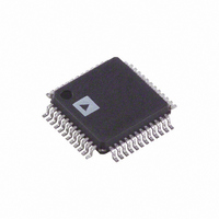
AD9763ASTZ Analog Devices Inc, AD9763ASTZ Datasheet - Page 18

AD9763ASTZ
Manufacturer Part Number
AD9763ASTZ
Description
IC DAC 10BIT DUAL 125MSPS 48LQFP
Manufacturer
Analog Devices Inc
Series
TxDAC+®r
Specifications of AD9763ASTZ
Data Interface
Parallel
Settling Time
35ns
Number Of Bits
10
Number Of Converters
2
Voltage Supply Source
Analog and Digital
Power Dissipation (max)
450mW
Operating Temperature
-40°C ~ 85°C
Mounting Type
Surface Mount
Package / Case
48-LQFP
Resolution (bits)
10bit
Sampling Rate
125MSPS
Input Channel Type
Parallel
Supply Voltage Range - Analog
3V To 5.5V
Supply Voltage Range - Digital
2.7V To 5.5V
Lead Free Status / RoHS Status
Lead free / RoHS Compliant
For Use With
AD9763-EBZ - BOARD EVAL FOR AD9763
Lead Free Status / RoHS Status
Lead free / RoHS Compliant, Lead free / RoHS Compliant
Available stocks
Company
Part Number
Manufacturer
Quantity
Price
Company:
Part Number:
AD9763ASTZ
Manufacturer:
ADI
Quantity:
180
Company:
Part Number:
AD9763ASTZ
Manufacturer:
Analog Devices Inc
Quantity:
10 000
Part Number:
AD9763ASTZ
Manufacturer:
ADI/亚德诺
Quantity:
20 000
Company:
Part Number:
AD9763ASTZRL
Manufacturer:
Analog Devices Inc
Quantity:
10 000
Part Number:
AD9763ASTZRL
Manufacturer:
ADI/亚德诺
Quantity:
20 000
AD9763
DAC OUTPUT CONFIGURATIONS
The following sections illustrate some typical output configura-
tions for the AD9763. Unless otherwise noted, it is assumed that
I
optimum dynamic performance, a differential output configura-
tion is suggested. A differential output configuration can consist
of either an RF transformer or a differential op amp configura-
tion. The transformer configuration provides the optimum high
frequency performance and is recommended for any application
allowing for ac coupling. The differential op amp configuration
is suitable for applications requiring dc coupling, a bipolar
output, signal gain, and/or level shifting, within the bandwidth
of the chosen op amp.
A single-ended output is suitable for applications requiring a
unipolar voltage output. A positive unipolar output voltage
results if I
sized load resistor (R
can be more suitable for a single-supply system requiring a
dc-coupled, ground referred output voltage. Alternatively, an
amplifier could be configured as an I-V converter, thus converting
I
provides the best dc linearity because I
at a virtual ground. Note that I
performance than I
DIFFERENTIAL COUPLING USING A
TRANSFORMER
An RF transformer can be used to perform a differential-to-
single-ended signal conversion as shown in Figure 35. A
differentially coupled transformer output provides the optimum
distortion performance for output signals whose spectral content
lies within the pass band of the transformer. An RF transformer
such as the Mini-Circuits® T1-1T provides excellent rejection of
common-mode distortion (that is, even-order harmonics) and
noise over a wide frequency range. It also provides electrical
isolation and the ability to deliver twice the power to the load.
Transformers with different impedance ratios can also be used
for impedance matching purposes. The transformer provides ac
coupling only.
OUTFS
OUTA
or I
is set to a nominal 20 mA. For applications requiring the
OUTB
AD9763
OUTA
Figure 35. Differential Output Using a Transformer
into a negative unipolar voltage. This configuration
and/or I
I
I
OUTA
OUTB
OUTB
LOAD
OUTB
.
B
) referred to ACOM. This configuration
B
is connected to an appropriately-
OPTIONAL
R
DIFF
OUTA
MINI-CIRCUITS
provides slightly better
T1-1T
OUTA
or I
OUTB
R
LOAD
is maintained
Rev. D | Page 18 of 32
The center tap on the primary side of the transformer must be
connected to ACOM to provide the necessary dc current path
for both I
at I
ACOM and should be maintained with the specified output
compliance range of the AD9763. A differential resistor (R
can be inserted in applications where the output of the trans-
former is connected to the load, R
filter or cable. R
transformer and provides the proper source termination that
results in a low VSWR. Approximately half the signal power is
dissipated across R
DIFFERENTIAL COUPLING USING AN OP AMP
An op amp can also be used to perform a differential-to-single-
ended conversion as shown in Figure 36. The AD9763 is
configured with two equal load resistors (R
differential voltage developed across I
to a single-ended signal via the differential op amp configuration.
An optional capacitor can be installed across I
forming a real pole in a low-pass filter. The addition of this
capacitor also enhances the distortion performance of the op
amp by preventing the high slewing output of the DAC from
overloading the op amp input.
The common-mode rejection of this configuration is typically
determined by the resistor matching. In this circuit, the differ-
ential op amp circuit using the AD8047 is configured to provide
some additional signal gain. The op amp must operate from a
dual supply because its output is approximately ±1.0 V. Select a
high speed amplifier that is capable of preserving the differential
performance of the AD9763 and meets other system level
objectives (cost and power). Consider the differential gain, gain
setting resistor values, and full-scale output swing capabilities of
the op amp when optimizing this circuit.
OUTA
AD9763
and I
OUTA
Figure 36. DC Differential Coupling Using an Op Amp
I
I
OUTA
OUTB
OUTB
and I
DIFF
(V
DIFF
OUTB
25Ω
is determined by the impedance ratio of the
OUTA
.
. The complementary voltages appearing
B
and V
C
OPT
OUTB
25Ω
LOAD
) swing symmetrically around
225Ω
225Ω
via a passive reconstruction
OUTA
and I
500Ω
LOAD
OUTA
AD8047
) of 25 Ω. The
OUTB
500Ω
and I
B
is converted
OUTB
DIFF
,
)


