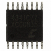
CS4341-CZZ Cirrus Logic Inc, CS4341-CZZ Datasheet - Page 22

CS4341-CZZ
Manufacturer Part Number
CS4341-CZZ
Description
IC DAC STER 24BIT 96KHZ 16TSSOP
Manufacturer
Cirrus Logic Inc
Datasheet
1.CS4341-CZZ.pdf
(34 pages)
Specifications of CS4341-CZZ
Data Interface
Serial
Number Of Bits
24
Number Of Converters
2
Voltage Supply Source
Single Supply
Power Dissipation (max)
90mW
Operating Temperature
-10°C ~ 70°C
Mounting Type
Surface Mount
Package / Case
16-TSSOP
Resolution (bits)
24bit
Sampling Rate
96kSPS
Input Channel Type
Serial
Supply Current
15mA
Digital Ic Case Style
TSSOP
No. Of Pins
16
Lead Free Status / RoHS Status
Lead free / RoHS Compliant
Settling Time
-
Lead Free Status / RoHS Status
Lead free / RoHS Compliant, Lead free / RoHS Compliant
Other names
598-1050-5
Available stocks
Company
Part Number
Manufacturer
Quantity
Price
Part Number:
CS4341-CZZ
Manufacturer:
CIRRUS
Quantity:
20 000
Company:
Part Number:
CS4341-CZZR
Manufacturer:
CILLUS
Quantity:
2 116
4.9.3a
4.9.3b
22
To write to the device, follow the procedure below while adhering to the control port Switching
Specifications in section 6.
1) Initiate a START condition to the I²C bus followed by the address byte. The upper 6 bits must
2) Wait for an acknowledge (ACK) from the part, then write to the memory address pointer, MAP.
3) Wait for an acknowledge (ACK) from the part, then write the desired data to the register point-
4) If the INCR bit (see section 4.9.2a) is set to 1, repeat the previous step until all the desired
5) If the INCR bit is set to 0 and further I²C writes to other registers are desired, it is necessary to
To read from the device, follow the procedure below while adhering to the control port Switching
Specifications. During this operation it is first necessary to write to the device, specifying the ap-
propriate register through the MAP.
1) After writing to the MAP (see section 4.9.3a), initiate a repeated START condition to the I²C
2) Signal the end of the address byte by not issuing an acknowledge. The device will then trans-
3) If the INCR bit is set to 1, the device will continue to transmit the contents of successive reg-
4) If the INCR bit is set to 0 and further I²C reads from other registers are desired, it is necessary
I²C Write
be 001000. The seventh bit must match the setting of the AD0 pin, and the eighth must be 0.
The eighth bit of the address byte is the R/W bit.
This byte points to the register to be written.
ed to by the MAP.
registers are written, then initiate a STOP condition to the bus.
repeat the procedure detailed from step 1. If no further writes to other registers are desired,
initiate a STOP condition to the bus.
I²C Read
bus followed by the address byte. The upper 6 bits must be 001000. The seventh bit must
match the setting of the AD0 pin, and the eighth must be 1. The eighth bit of the address byte
is the R/W bit.
mit the contents of the register pointed to by the MAP. The MAP will contain the address of the
last register written to the MAP.
isters. Continue providing a clock but do not issue an ACK on the bytes clocked out of the de-
vice. After all the desired registers are read, initiate a STOP condition to the bus.
to repeat the procedure detailed from step 1. If no further reads from other registers are de-
sired, initiate a STOP condition to the bus.
S D A
S C L
S tart
001000
AD0
Figure 22. I²C Write
W
ACK
MAP
1-8
ACK
DATA
1-8
ACK
Stop
CS4341
DS298F5


