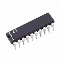
LTC1289BCN Linear Technology, LTC1289BCN Datasheet - Page 9

LTC1289BCN
Manufacturer Part Number
LTC1289BCN
Description
IC DATA ACQ SYS 12BIT 3V 20-DIP
Manufacturer
Linear Technology
Type
Data Acquisition System (DAS)r
Datasheet
1.LTC1289CCN.pdf
(28 pages)
Specifications of LTC1289BCN
Resolution (bits)
12 b
Sampling Rate (per Second)
25k
Data Interface
Serial, Parallel
Voltage Supply Source
Dual ±
Voltage - Supply
3V
Operating Temperature
0°C ~ 70°C
Mounting Type
Through Hole
Package / Case
20-DIP (0.300", 7.62mm)
Lead Free Status / RoHS Status
Contains lead / RoHS non-compliant
Available stocks
Company
Part Number
Manufacturer
Quantity
Price
Part Number:
LTC1289BCN#PBF
Manufacturer:
LINEAR/凌特
Quantity:
20 000
A
The LTC1289 is a data acquisition component which
contains the following functional blocks:
1. 12-bit successive approximation capacitive A/D
2. Analog multiplexer (MUX)
3. Sample-and-hold (S/H)
4. Synchronous, full duplex serial interface
5. Control and timing logic
DIGITAL CONSIDERATIONS
Serial Interface
The LTC1289 communicates with microprocessors and
other external circuitry via a synchronous, full duplex, four
wire serial interface (see Operating Sequence). The shift
clock (SCLK) synchronizes the data transfer with each bit
being transmitted on the falling SCLK edge and captured
on the rising SCLK edge in both transmitting and receiving
systems. The data is transmitted and received simulta-
neously (full duplex).
Data transfer is initiated by a falling chip select (CS) signal.
After the falling CS is recognized, an 8-bit input word is
shifted into the D
for the next conversion. Simultaneously, the result of the
D OUT
PPLICATI
SCLK
converter
D IN
CS
1
2
O
SHIFT CONFIGURATION
IN
3
U
input which configures the LTC1289
WORD IN
(Example: Differential Inputs (CH3-CH2), Bipolar, MSB-First and 12-Bit Word Length)
S
4
I FOR ATIO
5
U
6
7
8
W
t CYC
t SMPL
9
10
11
U
12
DON'T CARE
Operating Sequence
DON'T CARE
t CONV
D
D
previous conversion is output on the D
of the data exchange the requested conversion begins and
CS should be brought high. After t
complete and the results will be available on the next data
transfer cycle. As shown below, the result of a conversion
is delayed by one CS cycle from the input word requesting
it.
Input Data Word
The LTC1289 8-bit data word is clocked into the D
on the first eight rising SCLK edges after chip select is
recognized. Further inputs on the D
until the next CS cycle. The eight bits of the input word are
defined as follows:
IN
OUT
SGL/
DIFF
D
D
IN
OUT
TRANSFER
WORD 1
DATA
WORD 0
ODD/
SIGN
B11 B10 B9
MUX ADDRESS
(SB)
SELECT
CONVERSION
1
t
CONV
A/D
NEW CONFIGURATION WORD IN
B8
SHIFT A/D RESULT OUT AND
SELECT
B7 B6
0
D
D
IN
OUT
TRANSFER
WORD 2
UNIPOLAR/
DATA
BIPOLAR
WORD 1
B5
UNI
B4
CONV
IN
MSB-FIRST/
LSB-FIRST
CONVERSION
B3
pin are then ignored
MSBF
OUT
, the conversion is
t
CONV
A/D
B2
LTC1289
line. At the end
B1
WL1
D
D
LENGTH
B0
WORD
IN
OUT
WORD 3
IN
LTC1289 AI03
WORD 2
LTC1289 AI02
LTC1289 AI01
input
WL0
1289fb
9


