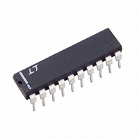
LTC1289BCN Linear Technology, LTC1289BCN Datasheet - Page 7

LTC1289BCN
Manufacturer Part Number
LTC1289BCN
Description
IC DATA ACQ SYS 12BIT 3V 20-DIP
Manufacturer
Linear Technology
Type
Data Acquisition System (DAS)r
Datasheet
1.LTC1289CCN.pdf
(28 pages)
Specifications of LTC1289BCN
Resolution (bits)
12 b
Sampling Rate (per Second)
25k
Data Interface
Serial, Parallel
Voltage Supply Source
Dual ±
Voltage - Supply
3V
Operating Temperature
0°C ~ 70°C
Mounting Type
Through Hole
Package / Case
20-DIP (0.300", 7.62mm)
Lead Free Status / RoHS Status
Contains lead / RoHS non-compliant
Available stocks
Company
Part Number
Manufacturer
Quantity
Price
Part Number:
LTC1289BCN#PBF
Manufacturer:
LINEAR/凌特
Quantity:
20 000
PI FU CTIO S
BLOCK DIAGRAM
CH0 – CH7 (Pins 1 – 8): Analog Inputs. The analog in-
puts must be free of noise with respect to AGND.
COM (Pin 9): Common. The common pin defines the zero
reference point for all single-ended inputs. It must be free
of noise and is usually tied to the analog ground plane.
DGND (Pin 10):Digital Ground. This is the ground for the
internal logic. Tie to the ground plane.
AGND (Pin 11): Analog Ground. AGND should be tied di-
rectly to the analog ground plane.
V
potential in the circuit. (Ground in single supply applica-
tions.)
REF
inputs must be kept free of noise with respect to AGND.
–
(Pin 12): Negative Supply. Tie V
U
–
, REF
U
+
(Pins 13,14) Reference Inputs. The reference
V
D
CC
IN
COM
CH0
CH1
CH2
CH3
CH4
CH5
CH6
CH7
20
17
U
1
2
3
4
5
6
7
8
9
DGND
10
INPUT MUX
REGISTER
ANALOG
INPUT
SHIFT
AGND
11
–
to the most negative
SAMPLE
HOLD
AND
V
–
12
COMP
REF
CAPACITIVE
CS (Pin 15): Chip Select Input. A logic low on this input
enables data transfer.
D
result is shifted out of this output.
D
shifted into this input.
SCLK (Pin 18): Shift Clock. This clock synchronizes the
serial data transfer.
ACLK (Pin 19): A/D Conversion Clock. This clock con-
trols the A/D conversion process.
V
free of noise and ripple by bypassing directly to the analog
ground plane.
CC
OUT
IN
13
12-BIT
–
DAC
(Pin 17): Digital Input. The A/D configuration word is
(Pin 20): Positive Supply. This supply must be kept
(Pin 16): Digital Data Output. The A/D conversion
REF
14
+
CONTROL
REGISTER
OUTPUT
TIMING
12-BIT
SHIFT
AND
SAR
LTC1289 BD
18
16
19
15
SCLK
ACLK
D
CS
OUT
LTC1289
1289fb
7


