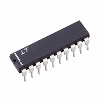
LTC1289BCN Linear Technology, LTC1289BCN Datasheet - Page 23

LTC1289BCN
Manufacturer Part Number
LTC1289BCN
Description
IC DATA ACQ SYS 12BIT 3V 20-DIP
Manufacturer
Linear Technology
Type
Data Acquisition System (DAS)r
Datasheet
1.LTC1289CCN.pdf
(28 pages)
Specifications of LTC1289BCN
Resolution (bits)
12 b
Sampling Rate (per Second)
25k
Data Interface
Serial, Parallel
Voltage Supply Source
Dual ±
Voltage - Supply
3V
Operating Temperature
0°C ~ 70°C
Mounting Type
Through Hole
Package / Case
20-DIP (0.300", 7.62mm)
Lead Free Status / RoHS Status
Contains lead / RoHS non-compliant
Available stocks
Company
Part Number
Manufacturer
Quantity
Price
Part Number:
LTC1289BCN#PBF
Manufacturer:
LINEAR/凌特
Quantity:
20 000
V
A “Quick Look” Circuit for the LTC1289
Users can get a quick look at the function and timing of the
LTC1289 by using the following simple circuit. REF
D
single-ended input, unipolar mode, MSB-first format and
16-bit word length. ACLK is driven by an external clock and
SCLK is driven by one half the clock rate. CS is driven at
1/128 the clock rate by the 74HC393 and D
data. All other pins are tied to a ground plane. The output
data from the D
which is set up to trigger on the falling edge of CS.
IN
TYPICAL
IN
are tied to V
DEGLITCHER
CHO
CH1
CH2
CH3
CH4
CH5
CH6
CH7
COM
DGND
Showing A/D Output of 010101010101 (555
Scope Trace of LTC1289 “Quick Look” Circuit
LTC1289
SCLK
ACLK
TIME
D
22µF
A “Quick Look” Circuit for the LTC1289
CS
OUT
AGND
ACLK
SCLK
D
A
REF
REF
V
OUT
D
OUT
CS
V
CC
IN
+
–
–
PPLICATI
CC
(B11)
MSB
pin can be viewed on an oscilloscope
OSCILLOSCOPE
selecting a 3V input span, CH7 as a
f/2
TO
VERTICAL: 5V/DIV
HORIZONTAL: 2µs/DIV
f
f/128
O
LSB
(B0)
CLOCK IN
2MHz MAX
A1
CLR1
1QA
1QB
1QC
1QD
GND
U
S
74HC393
ZEROES
FILLS
OUT
CLR2
2QA
2QB
2QC
2QD
V
CC
A2
HEX
outputs the
LTC1289 TA02
)
+
and
0.1µF
3.0V
SNEAK-A-BIT
The LTC1289’s unique ability to software select the polar-
ity of the differential inputs and the output word length is
used to achieve one more bit of resolution. Using the
circuit below with two conversions and some software, a
2’s complement 12-bit + sign word is returned to memory
inside the MPU. The MC68HC05C4 was chosen as an
example, however, any processor that operates at 3.3V
could be used.
Two 12-bit unipolar conversions are performed: the first
over a 0V to 2.5V span and the second over a 0V to –2.5V
span (by reversing the polarity of the inputs). The sign of
the input is determined by which of the two spans con-
tained it. Then the resulting number (ranging from –4095
to +4095 decimal) is converted to 2’s complement nota-
tion and stored in RAM.
OTHER CHANNELS
SNEAK-A-BIT is a trademark of Linear Technology Corp.
OR SNEAK-A-BIT
–2.5V TO +2.5V
V
IN
1ST CONVERSION
2ND CONVERSION
INPUTS
V
IN
(+) CH6
(–) CH7
(–) CH6
(+) CH7
TM
2.5V
CHO
CH1
CH2
CH3
CH4
CH5
CH6
CH7
COM
DGND
0V
LTC1289
SNEAK-A-BIT Circuit
–2.5V
0V
1ST CONVERSION
4096 STEPS
SNEAK-A-BIT
AGND
ACLK
SCLK
D
REF
REF
V
OUT
D
CS
CC
V
IN
+
–
–
2ND CONVERSION
4096 STEPS
0.1µF
22µF
SOFTWARE
–3.3V
10µF
LT1019
+3.3V
–2.5
–2.5V
1k
2.5V
LTC1289
0V
2MHz
ACLK
V
IN
SCLK
MOSI
MISO
CO
MC68HC05C4
23
8191 STEPS
LTC1289 TA04
LTC1289 TA03
1289fb


