HI7188IN Intersil, HI7188IN Datasheet - Page 20
HI7188IN
Manufacturer Part Number
HI7188IN
Description
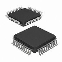
CONV A/D 16BIT 8:1 MUX 44-MQFP
Manufacturer
Intersil
Datasheet
1.HI7188IN.pdf
(24 pages)
Specifications of HI7188IN
Number Of Bits
16
Sampling Rate (per Second)
240
Data Interface
QSPI™, Serial, SPI™
Number Of Converters
1
Power Dissipation (max)
50mW
Voltage Supply Source
Analog and Digital, Dual ±
Operating Temperature
-40°C ~ 85°C
Mounting Type
Surface Mount
Package / Case
44-QFP
Lead Free Status / RoHS Status
Contains lead / RoHS non-compliant
Available stocks
Company
Part Number
Manufacturer
Quantity
Price


Control Register
The Control Register (CR) is 16 bits wide and contains
information that determines operating mode and the
system/chip level configuration. This configuration applies to
all logical channels and cannot be modified at the channel
level. Following are the bit assignments:
T3, T2, T1 - Bits 15, 14 and 13 are reserved and MUST
always be logic zero for normal operation. These bits are low
after RESET is applied.
CHOP. Bit 12 is the active low chop bit used to determine
whether the chopper stabilized amplifier is used or
bypassed. This bit is low (chop on) after RESET is applied.
SE. Bit 11 is the active high suppress EOS bit. If high, the
EOS interrupt will not go active when any logical channel is
in calibration mode. If this bit is high and no logical channels
are in the calibration mode, or this bit is low, EOS
functionality is as previously described. This bit allows the
user to suppress false EOS interrupts during calibration.
Only logical channels that are actively being converted are
considered. That is, if only two logical channels are being
converted but the CCR byte for a non active logical channel
is in a calibration mode, the EOS functionality is active. This
bit is low (suppress EOS off) after RESET is applied.
LNR. Bit 10 is the active high line noise rejection (LNR) bit. If
high LNR is selected. This bit is low (LNR off) after RESET is
applied.
FS. Bit 9 is the 50Hz/60Hz frequency select bit. If bit 9 is
high, the clock generation logic synchronizes conversions for
proper rejection of 50Hz line noise. If bit 9 is low, the clock
generation logic synchronizes conversions for proper
rejection of 60Hz line noise. This bit is low (60Hz LNR) after
RESET is applied.
TC. Bit 8 is the active high two’s complement bit used to
select between 2’s complementary and offset binary data
coding for bipolar mode. In bipolar mode, a high selects
two’s complement; when low data is offset binary. Note that
in unipolar mode the binary data coding is not affected by
the TC bit. This bit is low (offset binary data) after RESET is
applied.
N2, N1, N0. Bits 7, 6 and 5 are the bits that specify the number
of active logical channels to be converted. See Table 8. These
bits are low (one active channel) after RESET is applied.
MSB
MSB
N2
T3
N1
14
T2
6
CONTROL REGISTER BYTE 1
CONTROL REGISTER BYTE 0
N0
T1
13
5
CHOP
TP
12
4
20
SLP
SE
11
3
LNR
BD
10
2
MSB
FS
9
1
LSB
LSB
SDL
TC
HI7188
TP - Bit 4 is the active high two point calibration bit. When
high, the positive gain slope factor is used for both positive
and negative voltages. This bit is low (normal three point cal)
after RESET is applied.
SLP - Bit 3 is the active high sleep mode bit used to put the
device in a low power/standby mode. When high, conversion
stops and the conversion pointer is reset to logical channel
1. The four line noise rejection filters are cleared and EOS is
deactivated. The serial interface, calibration/data RAMs, CR
and CCR are not affected.
To return from sleep mode the user changes this bit from
high to low. This restarts the conversion process beginning
with logical channel 1. If line noise rejection is enabled, it
takes four complete scans (all active channels) to refill the
four line noise rejection filters before an EOS interrupt. If line
noise rejection not enabled, it takes 1 complete scan before
an EOS interrupt.
This bit is low (sleep mode off) after RESET is applied.
BD. Bit 2 is the byte direction bit used to determine either
ascending or descending order access for multi-byte
transfers. When high, ascending order is enabled. When low,
descending order is enabled. This bit is low (descending
order) after RESET is applied.
MSB. Bit 1 bit direction bit used to select whether a serial
data transfer is MSB or LSB first. When low, MSB first mode
is enabled while high selects LSB first. This bit is low (MSB
first) after RESET is applied.
SDL. Bit 0 selects a two-wire or three-wire transfer protocol of
the serial interface. When low, two-wire data transfers are done
using the SDIO pin. Both data in and out of the part is uses the
by-directional SDIO pin. When high, three-wire data transfers
are done using the SDIO and SDO pins. Data into the part uses
the SDIO pin while data out uses the SDO pin. This bit is low
(two-wire, SDIO exclusively) after RESET is applied.
Channel Configuration Registers
The HI7188 Channel Configuration Registers (CCR) comprise
a 64-bit memory element that defines the logical channel
conversion order as well as each logical channel specific data
such as physical channel address, mode, gain, and
N2, N1, N0 CR [7:5]
TABLE 8. NUMBER OF CONVERSION CHANNELS
000
001
010
011
100
101
110
111
NUMBER OF CHANNELS TO CONVERT
1
2
3
4
5
6
7
8
Related parts for HI7188IN
Image
Part Number
Description
Manufacturer
Datasheet
Request
R

Part Number:
Description:
8-channel, 16-bit, High Precision, Sigma-delta A/d Sub-system
Manufacturer:
Intersil Corporation
Datasheet:
Part Number:
Description:
Intersil Corporation [CMOS Serial Controller Interface]
Manufacturer:
Intersil Corporation
Datasheet:
Part Number:
Description:
Manufacturer:
Intersil Corporation
Datasheet:
Part Number:
Description:
357-036-542-201 CARDEDGE 36POS DL .156 BLK LOPRO
Manufacturer:
Intersil Corporation
Datasheet:
Part Number:
Description:
1024-Word x 4-Bit LSI Static RAM
Manufacturer:
Intersil Corporation
Datasheet:
Part Number:
Description:
General Purpose NPN Transistor Arrays FN341.4
Manufacturer:
Intersil Corporation
Datasheet:
Part Number:
Description:
CMOS 16-Bit Microprocessor
Manufacturer:
Intersil Corporation
Datasheet:
Part Number:
Description:
Manufacturer:
Intersil Corporation
Datasheet:
Part Number:
Description:
Manufacturer:
Intersil Corporation
Datasheet:
Part Number:
Description:
Manufacturer:
Intersil Corporation
Datasheet:
Part Number:
Description:
Manufacturer:
Intersil Corporation
Datasheet:
Part Number:
Description:
CMOS 6-Bit Latch and Decoder Memory Interfaces
Manufacturer:
Intersil Corporation
Datasheet:
Part Number:
Description:
CA3046General Purpose NPN Transistor Arrays
Manufacturer:
Intersil Corporation
Datasheet:
Part Number:
Description:
Manufacturer:
Intersil Corporation
Datasheet:
Part Number:
Description:
TR909 DLC/FLC SLIC with Low Power Standby
Manufacturer:
Intersil Corporation
Datasheet: