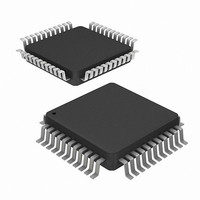
HI7188IN Intersil, HI7188IN Datasheet

HI7188IN
Specifications of HI7188IN
Available stocks
Related parts for HI7188IN
HI7188IN Summary of contents
Page 1
... AN9610 “Interfacing the HI7188 to a Microcontroller” - AN9538 “Using the HI7188 Serial Interface Ordering Information PART TEMP. o NUMBER RANGE ( HI7188IN - HI7188EVAL 25 CAUTION: These devices are sensitive to electrostatic discharge; follow proper IC Handling Procedures. | Intersil and Design is a trademark of Intersil Corporation. HI7188 File Number 4016 ...
Page 2
Pinouts OSC OSC DV DGND INL1 V INH1 V INL2 V INH2 V INL3 2 HI7188 HI7188 (MQFP) TOP VIEW ...
Page 3
Functional Block Diagram RHI RLO PHYSICAL CHANNELS V IN1H V IN2H V IN3H V IN4H V IN5H V IN6H V IN7H V IN8H INTEGRATING 4TH 1 ORDER PGIA MODULATOR V IN1L V IN2L V IN3L PGIA ...
Page 4
... CHANNEL CHANNEL CHANNEL CHANNEL CHANNEL CHANNEL CHANNEL CHANNEL 8 - -5V 4 HI7188 3.6864MHz 1 26 OSC 0 HI7188IN 25 +2.5V V RHI REFERENCE 24 V RLO 8 V INH1 7 V INL1 10 V INH2 9 V INL2 12 V INH3 11 V INL3 14 V INH4 13 V INL4 15 V INH5 14 V INL5 ...
Page 5
Pin Descriptions 44 LEAD MQFP PIN NAME 41 MODE Mode input. Used to select between Synchronous Self Clocking (MODE = 1) or Synchronous External Clocking (MODE = 0) for the Serial Port. 42 SCLK Serial interface clock. Synchronizes serial data ...
Page 6
Absolute Maximum Ratings Supply Voltage ...
Page 7
Electrical Specifications AV DD OSC IN PARAMETER TIMING CHARACTERISTICS SCLK Minimum Cycle Time, t SCLK SCLK Minimum Pulse Width, t SCLKPW CS to SCLK Precharge Time, t PRE Data Setup to SCLK Rising Edge (Write), t DSU Data Hold from ...
Page 8
Test Circuits ESD HUMAN BODY MACHINE MODEL C = 100pF ESD C ESD R = 10M 10M 1. FIGURE 2. HUMAN BODY AND MACHINE ...
Page 9
Waveforms (Continued) CS SCLK SDIO SDO t ACC EOS CS SCLK SDIO 1 Definitions Integral Non-Linearity (INL) - This is the maximum deviation of any digital code from a straight line passing through the endpoints of the transfer function. The ...
Page 10
Functional Description The HI7188 contains a differential 8 channel multiplexer, Programmable Gain Instrumentation Amplifier (PGIA), 4th order sigma-delta ADC, integrating filter, line noise rejection filters, Calibration and data RAMs, bidirectional serial port, clock oscillator, and a microsequencer. The 8 to ...
Page 11
INITIAL SYSTEM START PROGRAM THE SYSTEM LEVEL INFORMATION IN THE CONTROL REGISTER (CR) APPLY A ZERO SCALE INPUT TO EACH OF THE CHANNELS PROGRAM THE CHANNEL LEVEL INFORMATION IN THE CHANNEL CONFIGURATION REGISTERS (CCR) AND PLACE EACH CHANNEL IN ...
Page 12
Where C is the internal sampling capacitance and F S modulator sampling rate set by the master clock divided by six (F = 3.6864MHz/6 = 614.4kHz). S TABLE 2. EFFECTIVE INPUT IMPEDANCE vs GAIN SAMPLING SAMPLING RATE CAPACITOR GAIN (kHz) ...
Page 13
It is recommended that V be tied to analog ground when CM operating off +5V and also determines the headroom at the upper and lower ends of the power supplies which is limited by ...
Page 14
LOGICAL CHANNELS CH1 CH2 FROM ANALOG SECTION CH3 CH4 1 CH5 INTEGRATING CH6 FILTER 23 CH7 CH8 LOGICAL CHANNEL ADDRESS CCR REGISTERS A one channel example: 1. Channel 1 is sampled four times as labeled S1, S2, S3, and S4 ...
Page 15
The order of the gain calibrations is not important. Non-calibrated data can be obtained from the device by writing 000000 (h) to the Offset Calibration Register, 800000 ...
Page 16
System Negative Full Scale Calibration The system negative full scale calibration mode is a process that allows the user to lump negative gain errors of external circuitry and the internal gain errors of the HI7188 together to calculate the negative ...
Page 17
RAM0 and RAM1. The RAMs are configured such that when one is internally writable the other is readable via serial I/O. The following paragraphs describe the data RAM operation. Please refer to the Functional Block Diagram. For example, from initialization, ...
Page 18
Serial Interface The HI7188 has a flexible, synchronous serial communication port to allow easy interfacing to most industry standard microcontrollers and microprocessors. The serial I/O is compatible with most synchronous transfer formats, including both the Motorola 6805/11, SPI and Intel ...
Page 19
Detailed Register Descriptions Instruction Register The instruction register bit register which is used during a communications cycle for setting up read/write operations. Below are the bit assignments. INSTRUCTION REGISTER (BYTE) MSB R/W NB1 ...
Page 20
Control Register The Control Register (CR bits wide and contains information that determines operating mode and the system/chip level configuration. This configuration applies to all logical channels and cannot be modified at the channel level. Following are the ...
Page 21
The 64 bits are divided into two 32 bit register blocks referred to as CCR#2 and CCR#1. Each register contains four bytes pertaining to four logical channels. The register may be accessed bytes ...
Page 22
CS. Chip Select. This signal is an active low input that allows more than one device on the same serial communication lines. The SDO and SDIO will high impedance state when this signal is high. If driven ...
Page 23
Die Characteristics DIE DIMENSIONS: 215 mils x 257 mils (5466 m x 6536 m) METALLIZATION: Type: AlSiCu Å Thickness:Metal 2 16k Å Metal 1 6k SUBSTRATE POTENTIAL Metallization Mask Layout 23 HI7188 PASSIVATION: Type: Sandwich Å Nitride Thickness: ...
Page 24
... Accordingly, the reader is cautioned to verify that data sheets are current before placing orders. Information furnished by Intersil is believed to be accurate and reliable. However, no responsibility is assumed by Intersil or its subsidiaries for its use; nor for any infringements of patents or other rights of third parties which may result from its use ...


