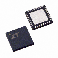
LTC2351HUH-14#PBF Linear Technology, LTC2351HUH-14#PBF Datasheet - Page 8

LTC2351HUH-14#PBF
Manufacturer Part Number
LTC2351HUH-14#PBF
Description
IC ADC 14BIT 1.5MSPS 32-QFN
Manufacturer
Linear Technology
Datasheet
1.LTC2351IUH-14PBF.pdf
(20 pages)
Specifications of LTC2351HUH-14#PBF
Number Of Bits
14
Sampling Rate (per Second)
1.5M
Data Interface
Serial, SPI™
Number Of Converters
1
Power Dissipation (max)
16.5mW
Voltage Supply Source
Single Supply
Operating Temperature
-40°C ~ 125°C
Mounting Type
Surface Mount
Package / Case
32-WFQFN Exposed Pad
Lead Free Status / RoHS Status
Lead free / RoHS Compliant
Available stocks
Company
Part Number
Manufacturer
Quantity
Price
LTC2351-14
PIN FUNCTIONS
V
plies 3V to the logic section. Bypass to DGND pin and
solid analog ground plane with a 10μF ceramic capacitor
(or 10μF tantalum in parallel with 0.1μF ceramic). Keep
in mind that internal digital output signal currents fl ow
through this pin. Care should be taken to place the 0.1μF
bypass capacitor as close to Pin 25 as possible. Pin 25
must be tied to Pin 24.
SEL2 (Pin 26): Most Signifi cant Bit Controlling the
Number of Channels Being Converted. In combination
with SEL1 and SEL0, 000 selects just the fi rst channel
(CH0) for conversion. Incrementing SELx selects addi-
tional channels(CH0–CH5) for conversion. 101, 110 or 111
select all six channels for conversion. Must be kept in a
fi xed state during conversion and during the subsequent
conversion to read data.
SEL1 (Pin 27): Middle Signifi cant Bit Controlling the
Number of Channels Being Converted. In combination
with SEL0 and SEL2, 000 selects just the fi rst channel
(CH0) for conversion. Incrementing SELx selects additional
channels for conversion. 101, 110 or 111 select all six
channels (CH0–CH5) for conversion. Must be kept in a
fi xed state during conversion and during the subsequent
conversion to read data.
SEL0 (Pin 28): Least Signifi cant Bit Controlling the
Number of Channels Being Converted. In combination
with SEL1 and SEL2, 000 selects just the fi rst channel
(CH0) for conversion. Incrementing SELx selects addi-
tional channels for conversion. 101, 110 or 111 select all
six channels (CH0–CH5) for conversion. Must be kept in
8
DD
(Pin 25): 3V Positive Digital Supply. This pin sup-
a fi xed state during conversion and during the subsequent
conversion to read data.
BIP (Pin 29): Bipolar/Unipolar Mode. The input dif-
ferential range is 0V – 2.5V when BIP is LOW, and it is
±1.25V when BIP is HIGH. Must be kept in fi xed state
during conversion and during subsequent conversion to
read data. When changing BIP between conversions the
full acquisition time must be allowed before starting the
next conversion. The output data is in 2’s complement
format for bipolar mode and straight binary format for
unipolar mode.
CONV (Pin 30): Convert Start. Holds the six analog input
signals and starts the conversion on the rising edge. Two
CONV pulses with SCK in fi xed HIGH or fi xed LOW state
starts nap mode. Four or more CONV pulses with SCK in
fi xed HIGH or fi xed LOW state starts sleep mode.
DGND (Pin 31): Digital Ground. This ground pin must be
tied directly to the solid ground plane. Digital input signal
currents fl ow through this pin.
SCK (Pin 32): External Clock Input. Advances the con-
version process and sequences the output data at SD0
(Pin1) on the rising edge. One or more SCK pulses wake
from sleep or nap power saving modes. 16 clock cycles
are needed for each of the channels that are activated by
SELx (Pins 26, 27, 28), up to a total of 96 clock cycles
needed to convert and read out all six channels.
Exposed Pad (Pin 33): GND. Must be tied directly to the
solid ground plane.
235114fb


