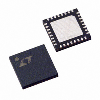
LTC2351HUH-14#PBF Linear Technology, LTC2351HUH-14#PBF Datasheet

LTC2351HUH-14#PBF
Specifications of LTC2351HUH-14#PBF
Available stocks
Related parts for LTC2351HUH-14#PBF
LTC2351HUH-14#PBF Summary of contents
Page 1
... Multiphase Power Measurement n Multiphase Motor Control n Data Acquisition Systems n Uninterruptable Power Supplies L, LT, LTC and LTM are registered trademarks of Linear Technology Corporation. All other trademarks are the property of their respective owners. Protected by U.S. Patents, including 6084440, 6522187. BLOCK DIAGRAM – + – ...
Page 2
... LTC2351CUH-14#PBF LTC2351CUH-14#TRPBF LTC2351IUH-14#PBF LTC2351IUH-14#TRPBF LTC2351HUH-14#PBF LTC2351HUH-14#TRPBF Consult LTC Marketing for parts specifi ed with wider operating temperature ranges. *The temperature grade is identifi label on the shipping container. For more information on lead free part marking, go to: For more information on tape and reel specifi cations, go to: CONVERTER CHARACTERISTICS temperature range, otherwise specifi ...
Page 3
ANALOG INPUT l The denotes the specifi cations which apply over the full operating temperature range, otherwise specifi cations are 25°C. With internal reference SYMBOL PARAMETER V Analog Differential Input Range (Notes ...
Page 4
LTC2351-14 DIGITAL INPUTS AND DIGITAL OUTPUTS full operating temperature range, otherwise specifi cations are Digital Input Current IN C Digital Input Capacitance IN V High Level Output Voltage OH V Low Level Output Voltage OL I Hi-Z ...
Page 5
TIMING CHARACTERISTICS Note 5: Integral linearity is tested with an external 2.55V reference and is defi ned as the deviation of a code from the straight line passing through the actual endpoints of a transfer curve. The deviation is measured ...
Page 6
LTC2351-14 TYPICAL PERFORMANCE CHARACTERISTICS 100kHz Unipolar Sine Wave 8192 Point FFT Plot 0 –10 –20 –30 –40 –50 –60 –70 –80 –90 –100 –110 –120 100 FREQUENCY (kHz) 235114 G06 Integral Linearity vs Output Code, Unipolar ...
Page 7
PIN FUNCTIONS SDO (Pin 1): Three-State Serial Data Output. Each set of six output data words represent the six analog input channels at the start of the previous conversion. Data for CH0 comes out fi rst and data for CH5 ...
Page 8
LTC2351-14 PIN FUNCTIONS V (Pin 25): 3V Positive Digital Supply. This pin sup- DD plies 3V to the logic section. Bypass to DGND pin and solid analog ground plane with a 10μF ceramic capacitor (or 10μF tantalum in parallel with ...
Page 9
BLOCK DIAGRAM + CH0 + 4 S & H – CH0 – CH1 + 7 S & H – CH1 – CH2 + 10 S & H – CH2 – ...
Page 10
LTC2351-14 TIMING DIAGRAMS SCK 10 235114fb ...
Page 11
TIMING DIAGRAMS SCK CONV NAP SLEEP V REF NOTE: NAP AND SLEEP ARE INTERNAL SIGNALS SCK SDO Nap Mode and Sleep Mode Waveforms t 1 SCK to SDO Delay SCK SDO V ...
Page 12
LTC2351-14 APPLICATIONS INFORMATION SELECTING THE NUMBER OF CONVERTED CHANNELS (SEL2, SEL1, SEL0) These three control pins select the number of channels being converted. 000 selects only the fi rst channel (CH0) for conversion. Incrementing SELx selects additional channels for conversion, ...
Page 13
... DC accuracy and settling time are most critical. The following list is a summary of the op amps that are suitable for driving the LTC2351-14. More detailed information is available in the Linear Technology Databooks and on the Web site at www.linear.com. LTC2351-14 LTC1566-1: Low Noise 2.3MHz Continuous Time Lowpass Filter ...
Page 14
LTC2351-14 APPLICATIONS INFORMATION INPUT FILTERING AND SOURCE IMPEDANCE The noise and the distortion of the input amplifi er and other circuitry must be considered since they will add to the LTC2351-14 noise and distortion. The small-signal bandwidth of the sample-and-hold ...
Page 15
APPLICATIONS INFORMATION INPUT SPAN VERSUS REFERENCE VOLTAGE The differential input range has a unipolar voltage span that equals the difference between the voltage at the reference buffer output V (Pin 23) and the voltage at REF ground. The differential input ...
Page 16
LTC2351-14 APPLICATIONS INFORMATION POWER-DOWN MODES Upon power-up, the LTC2351-14 is initialized to the active state and is ready for conversion. The nap and sleep mode waveforms show the power down modes for the LTC2351-14. The SCK and CONV inputs control ...
Page 17
APPLICATIONS INFORMATION and then buffer this signal with the appropriate number of inverters to drive the serial clock input of the processor serial port. Use the falling edge of the clock to latch data from the serial data output (SDO) ...
Page 18
LTC2351-14 APPLICATIONS INFORMATION HARDWARE INTERFACE TO TMS320C54x The LTC2351- serial output ADC whose interface has been designed for high speed buffered serial ports in fast digital signal processors (DSPs). Figure 7 shows an example of this interface using ...
Page 19
... ON THE TOP AND BOTTOM OF PACKAGE Information furnished by Linear Technology Corporation is believed to be accurate and reliable. However, no responsibility is assumed for its use. Linear Technology Corporation makes no representa- tion that the interconnection of its circuits as described herein will not infringe on existing patent rights. UH Package 32-Lead Plastic QFN (5mm × ...
Page 20
... LTC1666/LTC1667 12-/14-/16-Bit, 50Msps DAC LTC1668 References LT1460-2.5 Micropower Series Voltage Reference LT1461-2.5 Precision Voltage Reference LT1790-2.5 Micropower Series Reference in SOT-23 SoftSpan is a trademark of Linear Technology Corporation. Linear Technology Corporation 20 1630 McCarthy Blvd., Milpitas, CA 95035-7417 (408) 432-1900 FAX: (408) 434-0507 ● NC7SVU04P5X 0.1μ ...


