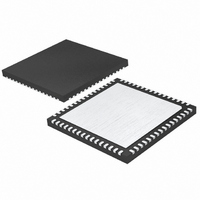
LTC2290IUP#PBF Linear Technology, LTC2290IUP#PBF Datasheet - Page 9

LTC2290IUP#PBF
Manufacturer Part Number
LTC2290IUP#PBF
Description
IC ADC DUAL 12BIT 10MSPS 64QFN
Manufacturer
Linear Technology
Datasheet
1.LTC2290CUPPBF.pdf
(24 pages)
Specifications of LTC2290IUP#PBF
Number Of Bits
12
Sampling Rate (per Second)
10M
Data Interface
Parallel
Number Of Converters
2
Power Dissipation (max)
138mW
Voltage Supply Source
Single Supply
Operating Temperature
-40°C ~ 85°C
Mounting Type
Surface Mount
Package / Case
64-WFQFN, Exposed Pad
Lead Free Status / RoHS Status
Lead free / RoHS Compliant
PI FU CTIO S
FUNCTIONAL BLOCK DIAGRA
SHDNA (Pin 59): Channel A Shutdown Mode Selection
Pin. Connecting SHDNA to GND and OEA to GND results
in normal operation with the outputs enabled. Connecting
SHDNA to GND and OEA to V
tion with the outputs at high impedance. Connecting
SHDNA to V
the outputs at high impedance. Connecting SHDNA to V
and OEA to V
high impedance.
MODE (Pin 60): Output Format and Clock Duty Cycle
Stabilizer Selection Pin. Note that MODE controls both
channels. Connecting MODE to GND selects offset binary
output format and turns the clock duty cycle stabilizer off.
1/3 V
clock duty cycle stabilizer on. 2/3 V
ment output format and turns the clock duty cycle stabilizer
U
SENSE
2.2µF
U
A
A
V
DD
IN
IN
CM
+
–
selects offset binary output format and turns the
U
INPUT
REFERENCE
S/H
DD
SELECT
RANGE
DD
1.5V
U
and OEA to GND results in nap mode with
results in sleep mode with the outputs at
BUF
U
REF
FIRST PIPELINED
ADC STAGE
DD
Figure 1. Functional Block Diagram (Only One Channel is Shown)
results in normal opera-
DD
AMP
SECOND PIPELINED
DIFF
REF
selects 2’s comple-
ADC STAGE
1µF
REFH
REFH
0.1µF
2.2µF
W
REFL
THIRD PIPELINED
REFL
ADC STAGE
DD
1µF
INTERNAL CLOCK SIGNALS
on. V
clock duty cycle stabilizer off.
V
Mode Bias. Bypass to ground with 2.2µF ceramic chip
capacitor. Do not connect to V
SENSEA (Pin 62): Channel A Reference Programming Pin.
Connecting SENSEA to V
and a ±0.5V input range. V
and a ±1V input range. An external reference greater than
0.5V and less than 1V applied to SENSEA selects an input
range of ±V
GND (Exposed Pad) (Pin 65): ADC Power Ground. The
Exposed Pad on the bottom of the package needs to be
soldered to ground.
CLOCK/DUTY
CMA
CONTROL
CYCLE
CLK
DD
FOURTH PIPELINED
(Pin 61): Channel A 1.5V Output and Input Common
ADC STAGE
selects 2’s complement output format and turns the
SENSEA
MODE
CONTROL
LOGIC
SHDN
. ±1V is the largest valid input range.
FIFTH PIPELINED
ADC STAGE
CMA
OE
DD
selects the internal reference
selects the internal reference
CMB
.
AND CORRECTION
SHIFT REGISTER
SIXTH PIPELINED
DRIVERS
OUTPUT
ADC STAGE
OGND
LTC2290
2290 F01
•
•
•
OF
D11
D0
2290fa
9
OV
DD


