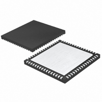
LTC2290IUP#PBF Linear Technology, LTC2290IUP#PBF Datasheet - Page 16

LTC2290IUP#PBF
Manufacturer Part Number
LTC2290IUP#PBF
Description
IC ADC DUAL 12BIT 10MSPS 64QFN
Manufacturer
Linear Technology
Datasheet
1.LTC2290CUPPBF.pdf
(24 pages)
Specifications of LTC2290IUP#PBF
Number Of Bits
12
Sampling Rate (per Second)
10M
Data Interface
Parallel
Number Of Converters
2
Power Dissipation (max)
138mW
Voltage Supply Source
Single Supply
Operating Temperature
-40°C ~ 85°C
Mounting Type
Surface Mount
Package / Case
64-WFQFN, Exposed Pad
Lead Free Status / RoHS Status
Lead free / RoHS Compliant
LTC2290
APPLICATIO S I FOR ATIO
Maximum and Minimum Conversion Rates
The maximum conversion rate for the LTC2290 is 10Msps.
For the ADC to operate properly, the CLK signal should
have a 50% (±10%) duty cycle. Each half cycle must have
at least 40ns for the ADC internal circuitry to have enough
settling time for proper operation.
An optional clock duty cycle stabilizer circuit can be used
if the input clock has a non 50% duty cycle. This circuit
uses the rising edge of the CLK pin to sample the analog
input. The falling edge of CLK is ignored and the internal
falling edge is generated by a phase-locked loop. The
input clock duty cycle can vary and the clock duty cycle
stabilizer will maintain a constant 50% internal duty cycle.
If the clock is turned off for a long period of time, the duty
cycle stabilizer circuit will require a hundred clock cycles
for the PLL to lock onto the input clock. To use the clock
duty cycle stabilizer, the MODE pin should be connected
to 1/3V
pin controls both Channel A and Channel B—the duty
cycle stabilizer is either on or off for both channels.
The lower limit of the LTC2290 sample rate is determined
by droop of the sample-and-hold circuits. The pipelined
architecture of this ADC relies on storing analog signals on
small valued capacitors. Junction leakage will discharge
the capacitors. The specified minimum operating fre-
quency for the LTC2290 is 1Msps.
DIGITAL OUTPUTS
Table 1. Output Codes vs Input Voltage
16
>+1.000000V
<–1.000000V
A
(2V Range)
+0.999512V
+0.999024V
+0.000488V
–0.000488V
–0.000976V
–0.999512V
–1.000000V
0.000000V
IN
+
– A
DD
IN
–
or 2/3V
OF
1
0
0
0
0
0
0
0
0
1
DD
U
using external resistors. The MODE
1111 1111 1111
1111 1111 1111
1111 1111 1110
1000 0000 0001
1000 0000 0000
0111 1111 1111
0111 1111 1110
0000 0000 0001
0000 0000 0000
0000 0000 0000
(Offset Binary)
D11 – D0
U
W
(2’s Complement)
0111 1111 1111
0111 1111 1111
0111 1111 1110
0000 0000 0001
0000 0000 0000
1111 1111 1111
1111 1111 1110
1000 0000 0001
1000 0000 0000
1000 0000 0000
D11 – D0
U
Digital Output Buffers
Figure 9 shows an equivalent circuit for a single output
buffer. Each buffer is powered by OV
lated from the ADC power and ground. The additional
N-channel transistor in the output driver allows operation
down to low voltages. The internal resistor in series with
the output makes the output appear as 50Ω to external
circuitry and may eliminate the need for external damping
resistors.
As with all high speed/high resolution converters, the digi-
tal output loading can affect the performance. The digital
outputs of the LTC2290 should drive a minimal capacitive
load to avoid possible interaction between the digital out-
puts and sensitive input circuitry. The output should be
buffered with a device such as an ALVCH16373 CMOS
latch. For full speed operation the capacitive load should
be kept under 10pF.
Lower OV
from the digital outputs.
LTC2290
LATCH
FROM
DATA
OE
PREDRIVER
LOGIC
DD
V
DD
voltages will also help reduce interference
Figure 9. Digital Output Buffer
V
DD
OV
DD
DD
and OGND, iso-
43Ω
2290 F09
OV
OGND
DD
TYPICAL
DATA
OUTPUT
0.1µF
0.5V
TO 3.6V
2290fa


