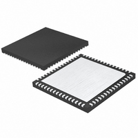
LTC2290IUP#PBF Linear Technology, LTC2290IUP#PBF Datasheet

LTC2290IUP#PBF
Specifications of LTC2290IUP#PBF
Related parts for LTC2290IUP#PBF
LTC2290IUP#PBF Summary of contents
Page 1
... A single-ended CLK input controls converter operation. An optional clock duty cycle stabilizer allows high perfor- mance at full speed for a wide range of clock duty cycles. , LTC and LT are registered trademarks of Linear Technology Corporation. All other trademarks are the property of their respective owners. Typical INL, 2V Range 1 ...
Page 2
LTC2290 ABSOLUTE AXI U RATI (Notes Supply Voltage (V ) ................................................. 4V DD Digital Output Ground Voltage (OGND) ....... –0. Analog Input Voltage (Note 3) ..... –0.3V ...
Page 3
ALOG I PUT The ● denotes the specifications which apply over the full operating temperature range, otherwise specifications are 25°C. (Note 4) A SYMBOL PARAMETER + V Analog Input Range (A – ...
Page 4
LTC2290 TER AL REFERE CE CHARACTERISTICS PARAMETER V Output Voltage CM V Output Tempco CM V Line Regulation CM V Output Resistance DIGITAL I PUTS A D DIGITAL OUTPUTS full operating temperature range, ...
Page 5
W U POWER REQUIRE E TS range, otherwise specifications are at T SYMBOL PARAMETER V Analog Supply Voltage DD OV Output Supply Voltage DD IV Supply Current DD P Power Dissipation DISS P Shutdown Power (Each Channel) SHDN P Nap ...
Page 6
LTC2290 W U TYPICAL PERFOR A CE CHARACTERISTICS Crosstalk vs Input Frequency –100 –105 –110 –115 –120 –125 –130 100 INPUT FREQUENCY (MHz) 2290 G01 8192 Point FFT 5.1MHz, IN –1dB, 2V Range ...
Page 7
W U TYPICAL PERFOR A CE CHARACTERISTICS SNR and SFDR vs Sample Rate, 2V Range 5MHz, –1dB IN 100 SAMPLE RATE (Msps) 2290 G10 I vs ...
Page 8
LTC2290 CTIO (Pin 1): Channel A Positive Differential Analog INA Input. – A (Pin 2): Channel A Negative Differential Analog INA Input. REFHA (Pins 3, 4): Channel A High Reference. Short together ...
Page 9
CTIO S SHDNA (Pin 59): Channel A Shutdown Mode Selection Pin. Connecting SHDNA to GND and OEA to GND results in normal operation with the outputs enabled. Connecting SHDNA to GND and OEA to V ...
Page 10
LTC2290 DIAGRA ANALOG N INPUT t H CLK – 5 D0-D11, OF ANALOG A INPUT A ANALOG B INPUT B t CLKA = CLKB = MUX A – ...
Page 11
U U APPLICATIO S I FOR ATIO DYNAMIC PERFORMANCE Signal-to-Noise Plus Distortion Ratio The signal-to-noise plus distortion ratio [S/(N + D)] is the ratio between the RMS amplitude of the fundamental input frequency and the RMS amplitude of all other ...
Page 12
LTC2290 U U APPLICATIO S I FOR ATIO applications, the analog inputs can be driven single-ended with slightly worse harmonic distortion. The CLK input is single-ended. The LTC2290 has two phases of operation, determined by the state of the CLK ...
Page 13
U U APPLICATIO S I FOR ATIO high to low, the inputs are reconnected to the sampling capacitors to acquire a new sample. Since the sampling capacitors still hold the previous sample, a charging glitch proportional to the change in ...
Page 14
LTC2290 U U APPLICATIO S I FOR ATIO Figure 4 demonstrates the use of a differential amplifier to convert a single ended input signal into a differential input signal. The advantage of this method is that it provides low frequency ...
Page 15
U U APPLICATIO S I FOR ATIO The difference amplifier generates the high and low refer- ence for the ADC. High speed switching circuits are connected to these outputs and they must be externally bypassed. Each output has two pins. ...
Page 16
LTC2290 U U APPLICATIO S I FOR ATIO Maximum and Minimum Conversion Rates The maximum conversion rate for the LTC2290 is 10Msps. For the ADC to operate properly, the CLK signal should have a 50% (±10%) duty cycle. Each half ...
Page 17
U U APPLICATIO S I FOR ATIO Data Format Using the MODE pin, the LTC2290 parallel digital output can be selected for offset binary or 2’s complement format. Note that MODE controls both Channel A and Channel B. Connecting MODE ...
Page 18
LTC2290 U U APPLICATIO S I FOR ATIO Digital Output Multiplexer The digital outputs of the LTC2290 can be multiplexed onto a single data bus. The MUX pin is a digital input that swaps the two data busses. If MUX ...
Page 19
U U APPLICATIO S I FOR ATIO W U LTC2290 2290fa 19 ...
Page 20
LTC2290 U U APPLICATIO S I FOR ATIO Silkscreen Top Top Side 2290fa ...
Page 21
U U APPLICATIO S I FOR ATIO W U Inner Layer 2 GND Inner Layer 3 Power LTC2290 2290fa 21 ...
Page 22
LTC2290 U U APPLICATIO S I FOR ATIO Bottom Side 2290fa ...
Page 23
... SHADED AREA IS ONLY A REFERENCE FOR PIN 1 LOCATION ON THE TOP AND BOTTOM OF PACKAGE 6. DRAWING NOT TO SCALE Information furnished by Linear Technology Corporation is believed to be accurate and reliable. However, no responsibility is assumed for its use. Linear Technology Corporation makes no represen- tation that the interconnection of its circuits as described herein will not infringe on existing patent rights Package 64-Lead Plastic QFN (9mm × ...
Page 24
... SNR, 9mm × 9mm QFN Package 150mW, 74.5dB SNR, 9mm × 9mm QFN Package 235mW, 74.4dB SNR, 9mm × 9mm QFN Package 400mW, 74.3dB SNR, 9mm × 9mm QFN Package www.linear.com ● 2290fa RD/LT 0106 REV A • PRINTED IN USA © LINEAR TECHNOLOGY CORPORATION 2004 ...


