LTC1415CSW#TR Linear Technology, LTC1415CSW#TR Datasheet - Page 19

LTC1415CSW#TR
Manufacturer Part Number
LTC1415CSW#TR
Description
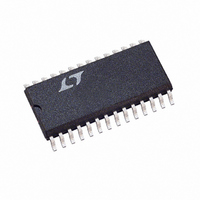
IC ADC 12BIT 1.25MSPS SMP 28SOIC
Manufacturer
Linear Technology
Datasheet
1.LTC1415CSWPBF.pdf
(24 pages)
Specifications of LTC1415CSW#TR
Number Of Bits
12
Sampling Rate (per Second)
1.25M
Data Interface
Parallel
Number Of Converters
1
Power Dissipation (max)
100mW
Voltage Supply Source
Single Supply
Operating Temperature
0°C ~ 70°C
Mounting Type
Surface Mount
Package / Case
28-SOIC (0.300", 7.50mm Width)
Lead Free Status / RoHS Status
Contains lead / RoHS non-compliant
Available stocks
Company
Part Number
Manufacturer
Quantity
Price
Timing and Control
Conversion start and data read operations are controlled
by three digital inputs: CONVST, CS and RD. A logic “0”
applied to the CONVST pin will start a conversion after the
ADC has been selected (i.e., CS is low). Once initiated, it
cannot be restarted until the conversion is complete.
Converter status is indicated by the BUSY output. BUSY
is low during a conversion.
Figures 16 through 20 show several different modes of
operation. In modes 1a and 1b (Figures 16 and 18) CS
and RD are both tied low. The falling edge of CONVST
starts the conversion. The data outputs are always enabled
and data can be latched with the BUSY rising edge. Mode
1a shows operation with a narrow logic low CONVST
pulse. Mode 1b shows a narrow logic high CONVST pulse.
In mode 2 (Figure 18) CS is tied low. The falling edge of the
CONVST signal again starts the conversion. Data outputs
are in three-state until read by the MPU with the RD signal.
Mode 2 can be used for operation with a shared MPU
databus.
A
PPLICATI
Figure 14b. SHDN to CONVST Wake-Up Timing
CONVST
SHDN
O
U
S
t
Figure 16. Mode 1a CONVST Starts a Conversion. Data Outputs Always Enabled
4
I FOR ATIO
U
CONVST
BUSY
DATA
W
DB11 TO DB0
DATA (N – 1)
t
6
1415 F14b
t
5
t
CONV
U
t
7
In slow memory and ROM modes (Figures 19 and 20) CS
is tied low and CONVST and RD are tied together. The MPU
starts the conversion and reads the output with the RD
signal. Conversions are started by the MPU or DSP (no
external sample clock).
In slow memory mode the processor applies a logic low to
RD (= CONVST), starting the conversion. BUSY goes low,
forcing the processor into a WAIT state. The previous
conversion result appears on the data outputs. When the
conversion is complete, the new conversion results ap-
pear on the data outputs; BUSY goes high, releasing the
processor and the processor takes RD (= CONVST) back
high and reads the new conversion data.
In ROM mode, the processor takes RD (= CONVST) low,
starting a conversion and reading the previous conversion
result. After the conversion is complete, the processor can
read the new result and initiate another conversion.
t
8
DB11 TO DB0
DATA N
CONVST
Figure 15. CS to CONVST Setup Timing
RD
CS
DB11 TO DB0
DATA (N + 1)
t
1
t
2
1415 • F16
LTC1415
1415 • F15
19


