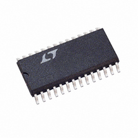
LTC1415CSW#TR Linear Technology, LTC1415CSW#TR Datasheet - Page 18

LTC1415CSW#TR
Manufacturer Part Number
LTC1415CSW#TR
Description
IC ADC 12BIT 1.25MSPS SMP 28SOIC
Manufacturer
Linear Technology
Datasheet
1.LTC1415CSWPBF.pdf
(24 pages)
Specifications of LTC1415CSW#TR
Number Of Bits
12
Sampling Rate (per Second)
1.25M
Data Interface
Parallel
Number Of Converters
1
Power Dissipation (max)
100mW
Voltage Supply Source
Single Supply
Operating Temperature
0°C ~ 70°C
Mounting Type
Surface Mount
Package / Case
28-SOIC (0.300", 7.50mm Width)
Lead Free Status / RoHS Status
Contains lead / RoHS non-compliant
Available stocks
Company
Part Number
Manufacturer
Quantity
Price
APPLICATIONS
LTC1415
DIGITAL INTERFACE
The A/D converter is designed to interface with micropro-
cessors as a memory mapped device. The CS and RD
control inputs are common to all peripheral memory
interfacing. A separate CONVST is used to initiate a
conversion.
Internal Clock
The A/D converter has an internal clock that eliminates the
need of synchronization between the external clock and
the CS and RD signals found in other ADCs. The internal
clock is factory trimmed to achieve a typical conversion
time of 0.70 s and a maximum conversion time over the
full operating temperature range of 0.75 s. No external
adjustments are required. The guaranteed maximum
acquisition time is 150ns. In addition, a throughput time of
800ns and a minimum sampling rate of 1.25Msps are
guaranteed.
Power Shutdown
The LTC1415 provides two power shutdown modes, Nap
and Sleep, to save power during inactive periods. The
18
U
INFORMATION
U
Figure 13d. Suggested Evaluation Circuit Board Solder Side Layout
W
U
Nap mode reduces the power by 87% and leaves only the
digital logic and reference powered up. The wake-up time
from Nap to active is 200ns. Follow the setup time shown
in Figure 14a to avoid inadvertently invoking Sleep mode.
In Sleep mode all bias currents are shut down and only
leakage current remains, about 1 A. Wake-up time from
Sleep mode is much slower since the reference circuit
must power up and settle to 0.01% for full 12-bit accu-
racy. Sleep mode wake-up time is dependent on the value
of the capacitor connected to the REFCOMP (Pin 4). The
wake-up time is 10ms with the recommended 10 F
capacitor. Shutdown is controlled by Pin 21 (SHDN); the
ADC is in shutdown when it is low. The shutdown mode is
selected with Pin 20 (NAP/SLP); high selects Nap.
NAP/SLP
SHDN
Figure 14a. NAP/SLP to SHDN Timing
t
3
1415 F14a


