LTC1415CSW#TR Linear Technology, LTC1415CSW#TR Datasheet - Page 15

LTC1415CSW#TR
Manufacturer Part Number
LTC1415CSW#TR
Description
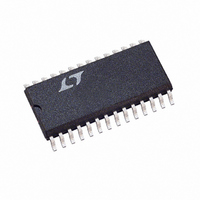
IC ADC 12BIT 1.25MSPS SMP 28SOIC
Manufacturer
Linear Technology
Datasheet
1.LTC1415CSWPBF.pdf
(24 pages)
Specifications of LTC1415CSW#TR
Number Of Bits
12
Sampling Rate (per Second)
1.25M
Data Interface
Parallel
Number Of Converters
1
Power Dissipation (max)
100mW
Voltage Supply Source
Single Supply
Operating Temperature
0°C ~ 70°C
Mounting Type
Surface Mount
Package / Case
28-SOIC (0.300", 7.50mm Width)
Lead Free Status / RoHS Status
Contains lead / RoHS non-compliant
Available stocks
Company
Part Number
Manufacturer
Quantity
Price
APPLICATIONS
width for these tracks should be as wide as possible. In
applications where the ADC data outputs and control
signals are connected to a continuously active micropro-
cessor bus, it is possible to get errors in the conversion
results. These errors are due to feedthrough from the
microprocessor to the successive approximation com-
parator. The problem can be eliminated by forcing the
microprocessor into a WAIT state during conversion or by
using three-state buffers to isolate the ADC data bus. The
traces connecting the pins and bypass capacitors must be
kept short and should be made as wide as possible.
The LTC1415 has differential inputs to minimize noise
coupling. Common mode noise on the + A
leads will be rejected by the input CMRR. The – A
can be used as a ground sense for the + A
LTC1415 will hold and convert the difference voltage
between + A
(Pin 2) should be kept as short as possible. In applications
where this is not possible, the + A
be run side by side to equalize coupling.
IN
and – A
U
IN
CIRCUITRY
. The leads to + A
ANALOG
INFORMATION
INPUT
U
IN
+
1
–
and – A
+A
+
W
IN
2
–A
IN
IN
10 F
Figure 12. Power Supply Grounding Practice
(Pin 1) and – A
IN
REFCOMP
traces should
IN
IN
4
0.1 F
U
input; the
and – A
ANALOG GROUND PLANE
IN
AGND
5
input
IN
IN
AV
+
LTC1415
DD
28
SUPPLY BYPASSING
High quality, low series resistance ceramic, 10 F bypass
capacitors should be used at the V
as shown in the Typical Application on the fist page of this
data sheet. Surface mount ceramic capacitors such as
Murata GRM235Y5V106Z016 provide excellent bypass-
ing in a small board space. Alternatively 10 F tantalum
capacitors in parallel with 0.1 F ceramic capacitors can be
used. Bypass capacitors must be located as close to the
pins as possible. The traces connecting the pins and the
bypass capacitors must be kept short and should be made
as wide as possible.
Example Layout
Figures 13a, 13b, 13c and 13d show the schematic and
layout of a suggested evaluation board. The layout demon-
strates the proper use of decoupling capacitors and ground
plane with a two layer printed circuit board.
10 F
DV
DD
27
0.1 F
OV
DD
26
DGND
14
OGND
19
DIGITAL
SYSTEM
DD
LTC1415 • F12
and REFCOMP pins
LTC1415
15


