ADC08D500CIYB/NOPB National Semiconductor, ADC08D500CIYB/NOPB Datasheet - Page 9

ADC08D500CIYB/NOPB
Manufacturer Part Number
ADC08D500CIYB/NOPB
Description
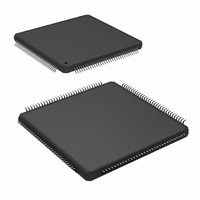
IC ADC 8BIT 500MSPS DUAL 128LQFP
Manufacturer
National Semiconductor
Series
PowerWise®r
Specifications of ADC08D500CIYB/NOPB
Number Of Bits
8
Sampling Rate (per Second)
500M
Data Interface
Serial
Number Of Converters
2
Power Dissipation (max)
1.78W
Voltage Supply Source
Single Supply
Operating Temperature
-40°C ~ 85°C
Mounting Type
Surface Mount
Package / Case
128-LQFP Exposed Pad
Lead Free Status / RoHS Status
Lead free / RoHS Compliant
Other names
*ADC08D500CIYB
*ADC08D500CIYB/NOPB
ADC08D500CIYB
*ADC08D500CIYB/NOPB
ADC08D500CIYB
Available stocks
Company
Part Number
Manufacturer
Quantity
Price
Company:
Part Number:
ADC08D500CIYB/NOPB
Manufacturer:
Texas Instruments
Quantity:
10 000
ANALOG INPUT AND REFERENCE CHARACTERISTICS
C
R
ANALOG OUTPUT CHARACTERISTICS
V
V
TC V
C
V
V
TC V
C
V
TEMPERATURE DIODE CHARACTERISTICS
∆V
CHANNEL-TO-CHANNEL CHARACTERISTICS
X-TALK
X-TALK
CLOCK INPUT CHARACTERISTICS
V
I
C
I
Symbol
Converter Electrical Characteristics
CMO
CMO_LVL
CMO
BG
BG
ID
IN
IN
LOAD
LOAD
IN
The following specifications apply after calibration for V
870mV
Floating, Non-Extended Control Mode, SDR Mode, R
tial. Boldface limits apply for T
BE
CMO
BG
P-P
, C
Analog Input Capacitance, Normal
operation (Notes 10, 11)
Analog Input Capacitance, DES
Mode (Notes 10, 11)
Differential Input Resistance
Common Mode Output Voltage
V
Coupling mode
Common Mode Output Voltage
Temperature Coefficient
Maximum V
Bandgap Reference Output
Voltage
Bandgap Reference Voltage
Temperature Coefficient
Maximum Bandgap Reference
Load Capacitance
Temperature Diode Voltage
Offset Error Match
Positive Full-Scale Error Match
Negative Full-Scale Error Match
Phase Matching (I,Q)
Crosstalk from I (Agressor) to Q
(Victim) Channel
Crosstalk from Q (Agressor) to I
(Victim) Channel
Differential Clock Input Level
Input Current
Input Capacitance (Notes 10, 11)
CMO
L
= 10 pF, Differential, a.c. coupled Sinewave Input Clock, f
input threshold to set DC
CMO
Parameter
load Capacitance
A
= T
MIN
to T
MAX
Differential
Each input pin to ground
Differential
Each input pin to ground
V
V
T
I
T
µA
192 µA vs. 12 µA,
T
192 µA vs. 12 µA,
T
Zero offset selected in Control
Register
Zero offset selected in Control
Register
F
Aggressor = 867 MHz F.S.
Victim = 100 MHz F.S.
Aggressor = 867 MHz F.S.
Victim = 100 MHz F.S.
Sine Wave Clock
Square Wave Clock
V
Differential
Each input to ground
BG
A
A
J
J
IN
A
A
IN
. All other limits T
= 25˚C
= 85˚C
= −40˚C to +85˚C
= −40˚C to +85˚C, I
= 1.8V
= 2.0V
=
= 1.0 GHz
= 0 or V
EXT
±
A
100 µA
= V
= 3300Ω
IN
DR
Conditions
(Continued)
9
= V
= +1.9V
A
±
A
0.1%, Analog Signal Source Impedance = 100Ω Differen-
= 25˚C, unless otherwise noted. (Notes 6, 7)
BG
DC
CLK
, OutV = 1.9V, V
=
= 500 MHz at 0.5V
±
100
(Note 8)
Typical
71.23
85.54
0.02
0.08
1.26
0.60
0.66
1.26
0.02
100
118
<
−71
-71
IN
1.6
2.2
0.6
0.6
1.5
±
28
1
1
1
1
1
FSR (a.c. coupled) = differential
P-P
with 50% duty cycle, V
(Note 8)
Limits
0.95
1.45
1.20
1.33
106
0.4
2.0
0.4
2.0
94
80
80
www.national.com
V
V
V
V
Ω (max)
(Limits)
V (max)
V (max)
P-P
P-P
Ω (min)
V (min)
ppm/˚C
V (min)
ppm/˚C
Degree
P-P
P-P
Units
LSB
LSB
LSB
mV
mV
pF
pF
pF
pF
pF
pF
dB
dB
µA
pF
pF
V
V
(max)
(max)
(min)
(min)
BG
=


