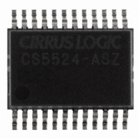
CS5524-ASZ Cirrus Logic Inc, CS5524-ASZ Datasheet - Page 34

CS5524-ASZ
Manufacturer Part Number
CS5524-ASZ
Description
IC ADC 24BIT 4CH 20SSOP
Manufacturer
Cirrus Logic Inc
Specifications of CS5524-ASZ
Number Of Converters
1
Package / Case
24-SSOP
Number Of Bits
24
Data Interface
Serial
Power Dissipation (max)
14.8mW
Voltage Supply Source
Analog and Digital
Operating Temperature
-40°C ~ 85°C
Mounting Type
Surface Mount
Number Of Adc Inputs
4
Architecture
Delta-Sigma
Conversion Rate
617 SPs
Resolution
24 bit
Input Type
Voltage
Interface Type
Serial (3-Wire)
Voltage Reference
2.5 V
Supply Voltage (max)
5 V
Supply Voltage (min)
25 mV
Maximum Power Dissipation
500 mW
Maximum Operating Temperature
+ 85 C
Mounting Style
SMD/SMT
Input Voltage
25 mV to 5 V
Minimum Operating Temperature
- 40 C
Lead Free Status / RoHS Status
Lead free / RoHS Compliant
For Use With
598-1012 - EVAL BOARD FOR CS5524 ADC
Lead Free Status / Rohs Status
Lead free / RoHS Compliant
Other names
598-1106-5
Available stocks
Company
Part Number
Manufacturer
Quantity
Price
Part Number:
CS5524-ASZ
Manufacturer:
CIRRUS
Quantity:
20 000
The variables are defined below.
2.3.3 Calibration Tips
Calibration steps are performed at the output word
rate selected by the WR2-WR0 bits of the configu-
ration register. Since higher word rates result in
conversion words with more peak-to-peak noise,
calibration should be performed at lower output
word rates. Also, to minimize digital noise near
the device, the user should wait for each calibration
step to be completed before reading or writing to
the serial port.
For maximum accuracy, calibrations should be per-
formed for offset and gain (selected by changing
the G2-G0 bits of the desired Setup). Note that only
one gain range can be calibrated per physical chan-
nel. If factory calibration of the user’s system is
performed using the system calibration capabilities
of the CS5521/22/23/24/28, the offset and gain reg-
ister contents can be read by the system microcon-
troller and recorded in EEPROM. These same
calibration words can then be uploaded into the off-
set and gain registers of the converter when power
is first applied to the system, or when the gain range
is changed.
34
V0
V1
Ru
Ru0 =
Ru1
Rc
Rc0
Rc1
Co
Cg
=
=
=
=
=
=
=
=
= Result of uncalibrated conversion of V1
First calibration voltage
Second calibration voltage (greater than V0)
Result of any uncalibrated conversion
Result of uncalibrated conversion V0
(24-bit integer or 2’s complement)
(24-bit integer or 2’s complement)
Result of any conversion
Desired calibrated result of converting V0
(24-bit integer or 2’s complement)
Desired calibrated result of converting V1
(24-bit integer or 2’s complement)
Offset calibration register value
Gain calibration register value
(24-bit integer)
(24-bit 2’s complement)
2.3.4 Limitations in Calibration Range
System calibration can be limited by signal head-
room in the analog signal path inside the chip as
discussed under the Analog Input section of this
data sheet. For gain calibration the full-scale input
signal can be reduced to the point in which the gain
register reaches its upper limit of (4-2
or FFFFFF (hexadecimal). Under nominal condi-
tions, this occurs with a full-scale input signal
equal to about 1/4 the nominal full scale. With the
converter’s intrinsic gain error, this full-scale input
signal may be higher or lower. In defining the min-
imum Full Scale Calibration Range (FSCR) under
ANALOG CHARACTERISTICS, margin is retained
to accommodate the intrinsic gain error. Alterna-
tively the input full-scale signal can be increased to
a point in which the modulator reaches its 1’s den-
sity limit of 80 percent, which under nominal con-
dition occurs when the full-scale input signal is 1.5
times the nominal full scale. With the chip’s intrin-
sic gain error, this full-scale input signal may be
higher or lower. In defining the maximum FSCR,
margin is again incorporated to accommodate the
intrinsic gain error. In addition, for full-scale inputs
greater than the nominal full-scale value of the
range selected, there is some voltage at which var-
ious internal circuits may saturate due to limited
amplifier headroom. This is most likely to occur in
the 100 mV range.
2.4 Performing Conversions and Reading
the Data Conversion FIFO
The CS5521/22/23/24/28 offers various modes of
performing conversions. The sections that follow
detail the differences between the conversion
modes. The sections also provide examples illus-
trating how to use the conversion modes with the
channel-setup registers and to acquire conversions
for further processing. While reading, note that the
CS5521/22 have a FIFO which is four words deep.
The CS5523/24 have a FIFO which is eight words
deep and the CS5528 has a FIFO which is sixteen
CS5521/22/23/24/28
-22
DS317F4
decimal)


