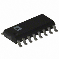
AD7888ARZ Analog Devices Inc, AD7888ARZ Datasheet - Page 9

AD7888ARZ
Manufacturer Part Number
AD7888ARZ
Description
IC ADC 12BIT 8CH SRL 16-SOIC
Manufacturer
Analog Devices Inc
Datasheet
1.AD7888ARZ.pdf
(17 pages)
Specifications of AD7888ARZ
Data Interface
DSP, MICROWIRE™, QSPI™, Serial, SPI™
Number Of Bits
12
Sampling Rate (per Second)
125k
Number Of Converters
1
Power Dissipation (max)
3.5mW
Voltage Supply Source
Single Supply
Operating Temperature
-40°C ~ 105°C
Mounting Type
Surface Mount
Package / Case
16-SOIC (0.154", 3.90mm Width)
Resolution (bits)
12bit
Sampling Rate
125kSPS
Input Channel Type
Single Ended
Supply Voltage Range - Analog
2.7V To 5.25V
Supply Current
700µA
Lead Free Status / RoHS Status
Lead free / RoHS Compliant
Available stocks
Company
Part Number
Manufacturer
Quantity
Price
Company:
Part Number:
AD7888ARZ
Manufacturer:
ADI
Quantity:
1 000
Part Number:
AD7888ARZ
Manufacturer:
ADI/亚德诺
Quantity:
20 000
Company:
Part Number:
AD7888ARZ-REEL7
Manufacturer:
ADI
Quantity:
1 000
REV. C
TYPICAL CONNECTION DIAGRAM
Figure 8 shows a typical connection diagram for the AD7888.
Both AGND pins are connected to the analog ground plane of
the system. V
provide an analog input range of 0 V to V
result is output in a 16-bit word with four leading zeroes fol-
lowed by the MSB of the 12-bit result. For applications where
power consumption is of concern, the automatic power down at
the end of conversion should be used to improve power perfor-
mance. See Modes of Operation section of the data sheet.
Analog Input
Figure 9 shows an equivalent circuit of the analog input structure
of the AD7888. The two diodes D1 and D2 provide ESD pro-
tection for the analog inputs. Care must be taken to ensure that
the analog input signal never exceeds the supply rails by more
than 200 mV. This will cause these diodes to become forward-
biased and start conducting current into the substrate. 20 mA is
the maximum current these diodes can conduct without causing
irreversible damage to the part. However, it is worth noting that
a small amount of current (1 mA) being conducted into the
substrate due to an overvoltage on an unselected channel, can
cause inaccurate conversions on a selected channel. The capaci-
tor C1 in Figure 9 is typically about 4 pF and can primarily be
attributed to pin capacitance. The resistor R1 is a lumped com-
ponent made up of the on resistance of a multiplexer and a switch.
This resistor is typically about 100 Ω. The capacitor C2 is the
ADC sampling capacitor and has a capacitance of 20 pF typically.
Note: The analog input capacitance seen when the track and
hold is in track mode is typically 38 pF, while in hold mode it is
typically 4 pF.
SUPPLY 2.7V
TO 5.25V
V
IN
REF OUT
REF IN/
REF
INPUT
0V TO
C1
4pF
is connected to a well decoupled V
10 F
V
DD
D1
D2
0.1 F
CONVERSION PHASE – SWITCH OPEN
AIN8
AGND
AGND
AIN1
AIN2
TRACK PHASE – SWITCH CLOSED
V
DD
AD7888
REF OUT
REF IN/
SCLK
DOUT
R1
DIN
CS
DD
SERIAL
INTERFACE
20pF
C2
. The conversion
DD
pin to
C/ P
For ac applications, removing high frequency components from
the analog input signal is recommended by use of an RC low-
pass filter on the relevant analog input pin. In applications
where harmonic distortion and signal to noise ratio are critical
the analog input should be driven from a low impedance source.
Large source impedances will significantly affect the ac perfor-
mance of the ADC. This may necessitate the use of an input
buffer amplifier. The choice of the op amp will be a function of
the particular application.
When no amplifier is used to drive the analog input the source
impedance should be limited to low values. The maximum
source impedance will depend on the amount of total harmonic
distortion (THD) that can be tolerated. The THD will increase
as the source impedance increases and performance will degrade.
Figure 10 shows a graph of the total harmonic distortion versus
analog input signal frequency for different source impedances.
Analog Input Selection
On power-up, the default AIN selection is AIN1. When returning
to normal operation from power-down, the AIN selected will be
the same one that was selected prior to power-down being initi-
ated. Table II below shows the multiplexer address correspond-
ing to each analog input from AIN1 to AIN8 for the AD7888.
ADD2
0
0
0
0
1
1
1
1
On-Chip Reference
The AD7888 has an on-chip 2.5 V reference. This reference can
be enabled or disabled by clearing or setting the REF bit in the
Control Register, respectively. If the on-chip reference is to
be used externally in a system, it must be buffered before it is
applied elsewhere. If an external reference is applied to the device,
the internal reference is automatically overdriven. However, in
–65
–70
–75
–80
–85
–90
0.15
THD vs. FREQUENCY FOR DIFFERENT
SOURCE IMPEDANCES
V
5V EXT REFERENCE
DD
ADD1
0
0
1
1
0
0
1
1
Table II. Channel Configurations
= 5V
10.89
R
INPUT FREQUENCY – kHz
IN
= 10 , C
ADD0
0
1
0
1
0
1
0
1
21.14
R
IN
IN
= 50 , C
= 10nF
31.59
R
IN
Analog Input Channel
AIN1
AIN2
AIN3
AIN4
AIN5
AIN6
AIN7
AIN8
IN
= 1k , C
= 2.2nF
42.14
AD7888
IN
= 100pF
49.86


