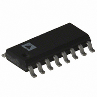
AD7888ARZ Analog Devices Inc, AD7888ARZ Datasheet - Page 12

AD7888ARZ
Manufacturer Part Number
AD7888ARZ
Description
IC ADC 12BIT 8CH SRL 16-SOIC
Manufacturer
Analog Devices Inc
Datasheet
1.AD7888ARZ.pdf
(17 pages)
Specifications of AD7888ARZ
Data Interface
DSP, MICROWIRE™, QSPI™, Serial, SPI™
Number Of Bits
12
Sampling Rate (per Second)
125k
Number Of Converters
1
Power Dissipation (max)
3.5mW
Voltage Supply Source
Single Supply
Operating Temperature
-40°C ~ 105°C
Mounting Type
Surface Mount
Package / Case
16-SOIC (0.154", 3.90mm Width)
Resolution (bits)
12bit
Sampling Rate
125kSPS
Input Channel Type
Single Ended
Supply Voltage Range - Analog
2.7V To 5.25V
Supply Current
700µA
Lead Free Status / RoHS Status
Lead free / RoHS Compliant
Available stocks
Company
Part Number
Manufacturer
Quantity
Price
Company:
Part Number:
AD7888ARZ
Manufacturer:
ADI
Quantity:
1 000
Part Number:
AD7888ARZ
Manufacturer:
ADI/亚德诺
Quantity:
20 000
Company:
Part Number:
AD7888ARZ-REEL7
Manufacturer:
ADI
Quantity:
1 000
AD7888
CS and the second rising edge of SCLK as shown in Figure 14a.
In microcontroller applications, this is readily achievable by
driving the CS input from one of the port lines and ensuring
that the serial data read (from the microcontrollers serial port) is
not initiated for 5 µs. In DSP applications, where the CS is
generally derived from the serial frame synchronization line, it is
not possible to separate the first falling edge and second rising
edge of SCLK after the CS falling edge by up to 5 µs. There-
fore, the user will need to write to the Control Register to exit
this mode and (by writing PM1 = 0 and PM0 = 0) put the part
into normal mode. A second conversion will then need to be
initiated when the part is powered up to obtain a conversion
result as shown in Figure 14b.
DOUT
SCLK
DIN
CS
DOUT
SCLK
DIN
CS
THE FIRST 8 CLOCKS. PM1 = 1 AND PM0 = 0
CONTROL REGISTER DATA IS LOADED ON
1
SHUTDOWN AT THE END
OF CONVERSION AS
PM1 = 1 AND PM0 = 0
THE PART ENTERS
4 LEADING ZEROES + CONVERSION RESULT
1
DATA IN
+ CONVERSION RESULT
DATA IN
THE FIRST 8 CLOCKS. PM1 = 1 AND PM0 = 1
CONTROL REGISTER DATA IS LOADED ON
4 LEADING ZEROES
8
16
STANDBY AT THE END OF
THE PART BEGINS TO POWER-
PM1 = 1 AND PM0 = 1
THE PART ENTERS
CONVERSION AS
UP FROM SHUTDOWN
16
1
DATA IN
+ CONVERSION RESULT
THE PART IN NORMAL MODE
PM1 AND PM0 = 0 TO PLACE
4 LEADING ZEROES
8
Autostandby (PM1 = 1, PM0 = 1)
In this mode, the AD7888 automatically enters a standby (or
sleep) mode at the end of every conversion. In this standby
mode, all on-chip circuitry, apart from the on-chip reference, is
powered down. This mode is similar to the autoshutdown but
in this case, the power-up time is much shorter as the on-chip
reference remains powered up at all times.
Figure 15 shows the general diagram of the operation of the
AD7888 in this mode. On the first falling SCLK edge after CS
goes low, the AD7888 comes out of standby. The AD7888
wake-up time is very short in this mode so it is possible to wake
up the part and carry out a valid conversion in the same read/
write operation. The input signal is sampled on the second
rising edge of SCLK following the CS falling edge. At the end
of conversion (last rising edge of SCLK) the part automatically
enters its standby mode.
THE PART REMAINS POWERED
FALLING EDGE AS PM1 = 1
FROM STANDBY ON SCLK
UP AS PM1 AND PM0 = 0
THE PART POWERS UP
16
1
AND PM0 = 1
4 LEADING ZEROES + CONVERSION RESULT
DATA IN
PM1 = 1 AND PM0 = 1 TO KEEP
1
DATA IN
THE PART IN THIS MODE
+ CONVERSION RESULT
PLACE THE PART BACK IN
4 LEADING ZEROES
AUTOSHUTDOWN MODE
PM1 = 1 AND PM0 = 0 TO
SHUTDOWN AT THE END OF
CONVERSION AS PM1 = 1
8
THE PART ENTERS
AND PM0 = 0
16
16
REV. C


