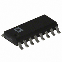
AD7888ARZ Analog Devices Inc, AD7888ARZ Datasheet - Page 13

AD7888ARZ
Manufacturer Part Number
AD7888ARZ
Description
IC ADC 12BIT 8CH SRL 16-SOIC
Manufacturer
Analog Devices Inc
Datasheet
1.AD7888ARZ.pdf
(17 pages)
Specifications of AD7888ARZ
Data Interface
DSP, MICROWIRE™, QSPI™, Serial, SPI™
Number Of Bits
12
Sampling Rate (per Second)
125k
Number Of Converters
1
Power Dissipation (max)
3.5mW
Voltage Supply Source
Single Supply
Operating Temperature
-40°C ~ 105°C
Mounting Type
Surface Mount
Package / Case
16-SOIC (0.154", 3.90mm Width)
Resolution (bits)
12bit
Sampling Rate
125kSPS
Input Channel Type
Single Ended
Supply Voltage Range - Analog
2.7V To 5.25V
Supply Current
700µA
Lead Free Status / RoHS Status
Lead free / RoHS Compliant
Available stocks
Company
Part Number
Manufacturer
Quantity
Price
Company:
Part Number:
AD7888ARZ
Manufacturer:
ADI
Quantity:
1 000
Part Number:
AD7888ARZ
Manufacturer:
ADI/亚德诺
Quantity:
20 000
Company:
Part Number:
AD7888ARZ-REEL7
Manufacturer:
ADI
Quantity:
1 000
REV. C
SERIAL INTERFACE
Figure 16 shows the detailed timing diagram for serial interfac-
ing to the AD7888. The serial clock provides the conversion
clock and also controls the transfer of information to and from
the AD7888 during conversion.
CS initiates the data transfer and conversion process. For the
autoshutdown mode, the first falling edge of SCLK after the
falling edge of CS wakes up the part. In all cases, it gates the
serial clock to the AD7888 and puts the on-chip track/hold into
track mode. The input signal is sampled on the second rising
edge of the SCLK input after the falling edge of CS. Thus, the
first one and one-half clock cycles after the falling edge of CS is
when the acquisition of the input signal takes place. This time is
denoted as the acquisition time (t
the acquisition time must allow for the wake-up time of 5 µs. The
on-chip track/hold goes from track mode to hold mode on the
second rising edge of SCLK and a conversion is also initiated on
this edge. The conversion process takes a further fourteen and
one-half SCLK cycles to complete. The rising edge of CS will
put the bus back into three-state. If CS is left low a new conver-
sion will be initiated.
The input channel that is sampled is the one selected in the
previous write to the Control Register. Thus, the user must
write ahead of the channel for conversion. In other words, the
user must write the channel address for the next conversion
while the present conversion is in progress.
DOUT
SCLK
DIN
CS
THREE-
STATE
t
t
2
1
DONTC
t
1
4
t
ACQ
t
5
ACQ
ZERO
). In autoshutdown mode,
2
4 LEADING ZEROS
t
6
ADD2
3
t
7
ADD1
4
ADD0
5
t
3
Writing of information to the Control Register takes place on
the first eight rising edges of SCLK in a data transfer. The Con-
trol Register is always written to when a data transfer takes
place. The user must be careful to always set up the correct
information on the DIN line when reading data from the part.
Sixteen serial clock cycles are required to perform the conver-
sion process and to access data from the AD7888. In applica-
tions where the first serial clock edge, following CS going low, is
a falling edge, this edge clocks out the first leading zero. Thus,
the first rising clock edge on the SCLK clock has the first lead-
ing zero provided. In applications where the first serial clock
edge, following CS going low, is a rising edge, the first leading
zero may not be set up in time for the processor to read it cor-
rectly. However, subsequent bits are clocked out on the falling
edge of SCLK so they are provided to the processor on the
following rising edge. Thus, the second leading zero is clocked
out on the falling edge subsequent to the first rising edge. The
final bit in the data transfer is valid on the 16th rising edge,
having being clocked out on the previous falling edge.
NOTE: The mark space ratio for SCLK is specified for at least
40% high time (with corresponding 60% low time) or 40% low
time (with corresponding 60% high time). As the SCLK frequency
is reduced, the mark space ratio may vary provided the conver-
sion time never exceeds 50 µs—to avoid capacitive droop effects.
DB11
t
CONVERT
REF
6
DB10
PM1
DB9
PM0
15
16
DB0
t
8
AD7888
THREE-
STATE


