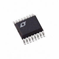
LTC1867LACGN#PBF Linear Technology, LTC1867LACGN#PBF Datasheet - Page 9

LTC1867LACGN#PBF
Manufacturer Part Number
LTC1867LACGN#PBF
Description
IC ADC 16BIT 8CH 175KSPS 16SSOP
Manufacturer
Linear Technology
Datasheet
1.LTC1863LCGNPBF.pdf
(16 pages)
Specifications of LTC1867LACGN#PBF
Number Of Bits
16
Sampling Rate (per Second)
175k
Data Interface
MICROWIRE™, Serial, SPI™
Number Of Converters
1
Power Dissipation (max)
2.7mW
Voltage Supply Source
Single Supply
Operating Temperature
0°C ~ 70°C
Mounting Type
Surface Mount
Package / Case
16-SSOP (0.150", 3.90mm Width)
Number Of Elements
1
Resolution
16Bit
Architecture
SAR
Sample Rate
175KSPS
Input Polarity
Unipolar/Bipolar
Input Type
Voltage
Rated Input Volt
2.5/±1.25V
Differential Input
Yes
Power Supply Requirement
Analog and Digital
Single Supply Voltage (typ)
3.3V
Single Supply Voltage (min)
2.7V
Single Supply Voltage (max)
3.6V
Dual Supply Voltage (typ)
Not RequiredV
Dual Supply Voltage (min)
Not RequiredV
Dual Supply Voltage (max)
Not RequiredV
Power Dissipation
2.7mW
Differential Linearity Error
-1LSB(Min)
Integral Nonlinearity Error
±3LSB
Operating Temp Range
0C to 70C
Operating Temperature Classification
Commercial
Mounting
Surface Mount
Pin Count
16
Package Type
SSOP N
Lead Free Status / RoHS Status
Lead free / RoHS Compliant
Available stocks
Company
Part Number
Manufacturer
Quantity
Price
APPLICATIONS INFORMATION
Overview
The LTC1863L/LTC1867L are complete, low power, multi-
plexed ADCs. They consist of a 12-/16-bit, 175ksps capaci-
tive successive approximation A/D converter, a precision
internal reference, a confi gurable 8-channel analog input
multiplexer (MUX) and a serial port for data transfer.
Conversions are started by a rising edge on the CS/CONV
input. Once a conversion cycle has begun, it cannot be
restarted. Between conversions, the ADCs receive an input
word for channel selection and output the conversion
result, and the analog input is acquired in preparation for
the next conversion. In the acquire phase, a minimum time
of 2.01μs will provide enough time for the sample-and-hold
capacitors to acquire the analog signal.
During the conversion, the internal differential 16-bit
capacitive DAC output is sequenced by the SAR from
the most signifi cant bit (MSB) to the least signifi cant bit
(LSB). The input is sucessively compared with the binary
weighted charges supplied by the differential capacitive
DAC. Bit decisions are made by a low power, differential
comparator that rejects common mode noise. At the end
of a conversion, the DAC output balances the analog input.
The SAR content (a 12-/16-bit data word) that represents
the analog input is loaded into the 12-/16-bit output latches.
Analog Input Multiplexer
The analog input multiplexer is controlled by a 7-bit input
data word. The input data word is defi ned as follows:
SD OS S1
SD = SINGLE/DIFFERENTIAL BIT
OS = ODD/SIGN BIT
S1 = ADDRESS SELECT BIT 1
S0 = ADDRESS SELECT BIT 0
COM = CH7/COM CONFIGURATION BIT
UNI = UNIPOLAR/BIPOLAR BIT
SLP = SLEEP MODE BIT
S0 COM UNI SLP
Tables 1 and 2 show the confi gurations when COM = 0,
and COM = 1.
Table 1. Channel Confi guration (When COM = 0, CH7/COM Pin
Is Used as CH7)
SD
0
0
0
0
0
0
0
0
1
1
1
1
1
1
1
1
OS
+
–
+
–
+
–
+
–
Changing the MUX Assignment “On the Fly”
0
0
0
0
1
1
1
1
0
0
0
0
1
1
1
1
+
–
+
–
(
(
(
(
(
(
(
(
–
+
–
+
–
+
–
+
{
{
)
)
)
)
)
)
)
)
+
+
+
+
+
+
+
{
{
{
{
7 Single-Ended
4 Differential
to CH7/COM
Examples of Multiplexer Options
1st Conversion
S1
CH2
CH3
CH4
CH5
CH7/COM
(UNUSED)
0
0
1
1
0
0
1
1
0
0
1
1
0
0
1
1
CH0
CH1
CH2
CH3
CH4
CH5
CH6
CH7/COM
CH0
CH1
CH2
CH3
CH4
CH5
CH6
LTC1863L/LTC1867L
CH7/COM (
S0
–
0
1
0
1
0
1
0
1
0
1
0
1
0
1
0
1
)
COM
0
0
0
0
0
0
0
0
0
0
0
0
0
0
0
0
Combinations of Differential
+
+
+
–
+
–
–
+
+
+
+
+
+
+
+
+
+
+
+
+
{
{
{
{
8 Single-Ended
and Single-Ended
2nd Conversion
CH0
CH1
CH2
CH3
CH4
CH5
CH6
CH7/COM
CH0
CH1
CH2
CH3
CH4
CH5
CH6
CH7/COM
GND (
CH7/COM (
GND (
CH2
CH3
CH4
CH5
Channel Confi guration
CH0
CH2
CH4
CH6
CH1
CH3
CH5
CH7
CH0
CH2
CH4
CH6
CH1
CH3
CH5
CH7
“+”
–
–
)
)
–
)
1863L7L AI02
1863L7L
GND
GND
GND
GND
GND
GND
GND
GND
“–”
CH0
CH4
CH6
CH1
CH3
CH5
CH7
CH2
1863l7lfc
9


