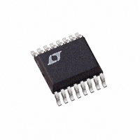
LTC1867LACGN#PBF Linear Technology, LTC1867LACGN#PBF Datasheet - Page 12

LTC1867LACGN#PBF
Manufacturer Part Number
LTC1867LACGN#PBF
Description
IC ADC 16BIT 8CH 175KSPS 16SSOP
Manufacturer
Linear Technology
Datasheet
1.LTC1863LCGNPBF.pdf
(16 pages)
Specifications of LTC1867LACGN#PBF
Number Of Bits
16
Sampling Rate (per Second)
175k
Data Interface
MICROWIRE™, Serial, SPI™
Number Of Converters
1
Power Dissipation (max)
2.7mW
Voltage Supply Source
Single Supply
Operating Temperature
0°C ~ 70°C
Mounting Type
Surface Mount
Package / Case
16-SSOP (0.150", 3.90mm Width)
Number Of Elements
1
Resolution
16Bit
Architecture
SAR
Sample Rate
175KSPS
Input Polarity
Unipolar/Bipolar
Input Type
Voltage
Rated Input Volt
2.5/±1.25V
Differential Input
Yes
Power Supply Requirement
Analog and Digital
Single Supply Voltage (typ)
3.3V
Single Supply Voltage (min)
2.7V
Single Supply Voltage (max)
3.6V
Dual Supply Voltage (typ)
Not RequiredV
Dual Supply Voltage (min)
Not RequiredV
Dual Supply Voltage (max)
Not RequiredV
Power Dissipation
2.7mW
Differential Linearity Error
-1LSB(Min)
Integral Nonlinearity Error
±3LSB
Operating Temp Range
0C to 70C
Operating Temperature Classification
Commercial
Mounting
Surface Mount
Pin Count
16
Package Type
SSOP N
Lead Free Status / RoHS Status
Lead free / RoHS Compliant
Available stocks
Company
Part Number
Manufacturer
Quantity
Price
LTC1863L/LTC1867L
APPLICATIONS INFORMATION
Total Harmonic Distortion
Total Harmonic Distortion (THD) is the ratio of the RMS
sum of all harmonics of the input signal to the fundamental
itself. The out-of-band harmonics alias into the frequency
band between DC and half the sampling frequency. THD
is expressed as:
where V
frequency and V
second through Nth harmonics.
Internal Reference
The LTC1863L and LTC1867L have an on-chip, temperature
compensated, curvature corrected, bandgap reference that
is factory trimmed to 1.25V. It is internally connected to
a reference amplifi er and is available at V
3k resistor is in series with the output so that it can be
easily overdriven by an external reference if better drift
and/or accuracy are required as shown in Figure 4. The
reference amplifi er gains the V
REFCOMP (Pin 9). This reference amplifi er compensation
12
Figure 4b. Using the LT1790A-1.25 as an External Reference
THD
1.25V
=
1
2.5V
20
is the RMS amplitude of the fundamental
Figure 4a. LTC1867L Reference Circuit
log
LT1790A-1.25
2.2μF
10μF
10
15
9
V
3V
2
IN
V
REFCOMP
GND
V
REF
through V
OUT
V
+
2
2
+
10μF
V
R3
3
REFERENCE
2
R2
V
N
AMP
+
2.2μF
0.1μF
1
REF
are the amplitudes of the
10
15
V
9
4
2
V
REFCOMP
GND
voltage by 2x to 2.5V at
REF
...
LTC1863L/
LTC1867L
LTC1863L/LTC1867L
R1
3k
+
V
1863L7L F04b
REFERENCE
N
BANDGAP
2
REF
1863L7L F04a
(Pin 10). A
pin, REFCOMP, must be bypassed with a 10μF ceramic or
tantalum in parallel with a 0.1μF ceramic for best noise
performance.
Digital Interface
The LTC1863L and LTC1867L have a very simple digital
interface that is enabled by the control input, CS/CONV.
A logic rising edge applied to the CS/CONV input will initi-
ate a conversion. After the conversion, taking CS/CONV
low will enable the serial port and the ADC will present
digital data in two’s complement format in bipolar mode
or straight binary format in unipolar mode, through the
SCK/SDO serial port.
Internal Clock
The internal clock is factory trimmed to achieve a typical
conversion time of 3.2μs and a maximum conversion time,
3.7μs, over the full operating temperature range. The typi-
cal acquisition time is 1.68μs, and a throughput sampling
rate of 175ksps is tested and guaranteed.
Automatic Nap Mode
The LTC1863L and LTC1867L go into automatic nap
mode when CS/CONV is held high after the conversion
is complete. With a typical operating current of 750μA
and automatic 170μA nap mode between conversions, the
power dissipation drops with reduced sample rate. The
ADC only keeps the V
when the part is in the automatic nap mode. The slower
the sample rate allows the power dissipation to be lower
(see Figure 5).
Figure 5. Supply Current vs f
800
700
600
500
400
300
200
100
1
V
DD
= 2.7V
REF
10
f
SAMPLE
and REFCOMP voltages active
(ksps)
100
1863L7L G09
SAMPLE
1000
1863l7lfc


