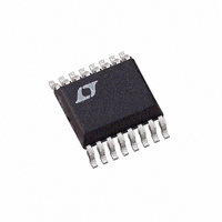
LTC1867LACGN#PBF Linear Technology, LTC1867LACGN#PBF Datasheet - Page 10

LTC1867LACGN#PBF
Manufacturer Part Number
LTC1867LACGN#PBF
Description
IC ADC 16BIT 8CH 175KSPS 16SSOP
Manufacturer
Linear Technology
Datasheet
1.LTC1863LCGNPBF.pdf
(16 pages)
Specifications of LTC1867LACGN#PBF
Number Of Bits
16
Sampling Rate (per Second)
175k
Data Interface
MICROWIRE™, Serial, SPI™
Number Of Converters
1
Power Dissipation (max)
2.7mW
Voltage Supply Source
Single Supply
Operating Temperature
0°C ~ 70°C
Mounting Type
Surface Mount
Package / Case
16-SSOP (0.150", 3.90mm Width)
Number Of Elements
1
Resolution
16Bit
Architecture
SAR
Sample Rate
175KSPS
Input Polarity
Unipolar/Bipolar
Input Type
Voltage
Rated Input Volt
2.5/±1.25V
Differential Input
Yes
Power Supply Requirement
Analog and Digital
Single Supply Voltage (typ)
3.3V
Single Supply Voltage (min)
2.7V
Single Supply Voltage (max)
3.6V
Dual Supply Voltage (typ)
Not RequiredV
Dual Supply Voltage (min)
Not RequiredV
Dual Supply Voltage (max)
Not RequiredV
Power Dissipation
2.7mW
Differential Linearity Error
-1LSB(Min)
Integral Nonlinearity Error
±3LSB
Operating Temp Range
0C to 70C
Operating Temperature Classification
Commercial
Mounting
Surface Mount
Pin Count
16
Package Type
SSOP N
Lead Free Status / RoHS Status
Lead free / RoHS Compliant
Available stocks
Company
Part Number
Manufacturer
Quantity
Price
LTC1863L/LTC1867L
APPLICATIONS INFORMATION
Table 2. Channel Confi guration (When COM = 1, CH7/COM Pin
Is Used as COMMON)
Driving the Analog Inputs
The analog inputs of the LTC1863L/LTC1867L are easy to
drive. Each of the analog inputs can be used as a single-
ended input relative to the GND pin (CH0-GND, CH1-GND,
etc) or in pairs (CH0 and CH1, CH2 and CH3, CH4 and CH5,
CH6 and CH7) for differential inputs. In addition, CH7 can
act as a COM pin for both single-ended and differential
modes if the COM bit in the input word is high. Regard-
less of the MUX confi guration, the “+” and “–” inputs are
sampled at the same instant. Any unwanted signal that is
common mode to both inputs will be reduced by the com-
mon mode rejection of the sample-and-hold circuit. The
inputs draw only one small current spike while charging
the sample-and-hold capacitors during the acquire mode.
In conversion mode, the analog inputs draw only a small
leakage current. If the source impedance of the driving
circuit is low then the LTC1863L/LTC1867L inputs can be
driven directly. More acquisition time should be allowed
for a higher impedance source.
The following list is a summary of the op amps that are
suitable for driving the LTC1863L/LTC1867L. More detailed
information is available in the Linear Technology data
books or Linear Technology website.
10
SD
Figure 1a. Optional RC Input Filtering for Single-Ended Input
1
1
1
1
1
1
1
OS
ANALOG
0
0
0
0
1
1
1
INPUT
S1
0
0
1
1
0
0
1
50Ω
S0
0
1
0
1
0
1
0
COM
2000pF
10μF
1
1
1
1
1
1
1
CHANNEL CONFIGURATION
CH0
GND
REFCOMP
LTC1863L/
LTC1867L
CH0
CH2
CH4
CH6
CH1
CH3
CH5
“+”
1863L7L F01a
CH7/COM
CH7/COM
CH7/COM
CH7/COM
CH7/COM
CH7/COM
CH7/COM
“–”
LT
LT1469: Dual LT1468
LT1490A/LT1491A: Dual/quad micropower amplifi ers,
50μA/amplifi er max, 500μV offset, common mode range
extends 44V above V
supplies.
LT1568: Very low noise, active RC fi lter building block,
cutoff frequency up to 10MHz, 2.7V to ±5V supplies.
LT1638/LT1639: Dual/quad 1.2MHz, 0.4V/μs amplifi ers,
230μA per amplifi er, 3V, 5V and ±15V supplies.
LT1881/LT1882: Dual and quad, 200pA bias current, rail-
to-rail output op amps, up to ±15V supplies.
LTC1992-2: Gain of 2 fully differential input/output am-
plifi er/driver, 2.5mV offset, C
supplies.
LT1995: 30MHz, 1000V/μs gain selectable amplifi er, pin
confi gurable as a difference amplifi er, inverting and non-
inverting amplifi er, ±2.5V to ±15V supplies.
LTC6912: Dual programmable gain amplifi ers with SPI
serial interface, 2mV offset, 2.7V to ±5V supplies.
LTC6915: Zero drift, instrumentation amplifi er with SPI
programmable gain, 125dB CMRR, 0.1% gain accuracy,
10μV offset.
Input Filtering
The noise and the distortion of the input amplifi er and
other circuitry must be considered since they will add to
the LTC1863L/LTC1867L noise and distortion. Noisy input
circuitry should be fi ltered prior to the analog inputs to
minimize noise. A simple 1-pole RC fi lter is suffi cient for
®
Figure 1b. Optional RC Input Filtering for Differential Inputs
1468: 90MHz, 22V/μs 16-bit accurate amplifi er
DIFFERENTIAL
ANALOG
INPUTS
50Ω
50Ω
–
independent of V
1000pF
1000pF
1000pF
10μF
LOAD
CH0
CH1
REFCOMP
stable, 2.7V to ±5V
LTC1863L/
+
LTC1867L
, 3V, 5V and ±15V
1863L7L F01b
1863l7lfc


