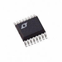
LTC1867LACGN#PBF Linear Technology, LTC1867LACGN#PBF Datasheet - Page 5

LTC1867LACGN#PBF
Manufacturer Part Number
LTC1867LACGN#PBF
Description
IC ADC 16BIT 8CH 175KSPS 16SSOP
Manufacturer
Linear Technology
Datasheet
1.LTC1863LCGNPBF.pdf
(16 pages)
Specifications of LTC1867LACGN#PBF
Number Of Bits
16
Sampling Rate (per Second)
175k
Data Interface
MICROWIRE™, Serial, SPI™
Number Of Converters
1
Power Dissipation (max)
2.7mW
Voltage Supply Source
Single Supply
Operating Temperature
0°C ~ 70°C
Mounting Type
Surface Mount
Package / Case
16-SSOP (0.150", 3.90mm Width)
Number Of Elements
1
Resolution
16Bit
Architecture
SAR
Sample Rate
175KSPS
Input Polarity
Unipolar/Bipolar
Input Type
Voltage
Rated Input Volt
2.5/±1.25V
Differential Input
Yes
Power Supply Requirement
Analog and Digital
Single Supply Voltage (typ)
3.3V
Single Supply Voltage (min)
2.7V
Single Supply Voltage (max)
3.6V
Dual Supply Voltage (typ)
Not RequiredV
Dual Supply Voltage (min)
Not RequiredV
Dual Supply Voltage (max)
Not RequiredV
Power Dissipation
2.7mW
Differential Linearity Error
-1LSB(Min)
Integral Nonlinearity Error
±3LSB
Operating Temp Range
0C to 70C
Operating Temperature Classification
Commercial
Mounting
Surface Mount
Pin Count
16
Package Type
SSOP N
Lead Free Status / RoHS Status
Lead free / RoHS Compliant
Available stocks
Company
Part Number
Manufacturer
Quantity
Price
TIMING CHARACTERISTICS
range, otherwise specifi cations are at T
Note 4: When these pin voltages are taken below GND, they will be
clamped by internal diodes. This product can handle input currents of
greater than 100mA below GND without latchup. These pins are not
clamped to V
Note 5: V
t
Note 6: Linearity, offset and gain error specifi cations apply for both
unipolar and bipolar modes. The INL and DNL are tested in bipolar mode.
Note 7: Integral nonlinearity is defi ned as the deviation of a code from a
straight line passing through the actual endpoints of the transfer curve.
The deviation is measured from the center of the quantization band.
Note 8: Unipolar offset is the offset voltage measured from +1/2LSB
when the output code fl ickers between 0000 0000 0000 0000 and
0000 0000 0000 0001 for LTC1867L and between 0000 0000 0000
TYPICAL PERFORMANCE CHARACTERISTICS
(LTC1867L)
r
= t
–100
–120
–140
–0.5
–1.0
–1.5
–2.0
–20
–40
–60
–80
f
2.0
1.5
1.0
0.5
= 5ns and V
0
0
0
0
4096 Points FFT Plot
(V
Integral Nonlinearity
vs Output Code
DD
V
f
SAMPLE
DD
DD
= 2.7V, f
DD
= 2.7V
= 3V, REFCOMP = Ext 3V)
21.875
.
16384
= 175ksps
IN
–
SAMPLE
FREQUENCY (kHz)
= 1.25V for bipolar mode unless otherwise specifi ed.
OUTPUT CODE
32768
43.75
= 175ksps and f
f
f
SNR = 84.7dB
SINAD = 83.5dB
THD = 90dB
SAMPLE
IN
= 1kHz
65.625
49152
= 175ksps
1863L7L G04
1863L7L G01
SCK
65536
A
87.5
= 25°C. (Note 5)
= 20MHz at 25°C,
–100
–110
–120
–130
–140
–0.5
–1.0
–1.5
–2.0
–60
–70
–80
–90
2.0
1.5
1.0
0.5
0
The
0.1
0
Differential Nonlinearity
vs Output Code
Crosstalk vs Input Frequency
V
f
V
f
SAMPLE
ACTIVE CHANNEL INPUT FREQUENCY (kHz)
SAMPLE
DD
DD
●
= 2.7V
= 3V
denotes the specifi cations which apply over the full operating temperature
16384
= 175ksps
= 175ksps
1
OUTPUT CODE
ADJACENT PAIR
32768
10
and 0000 0000 0001 for LTC1863L. Bipolar offset is the offset voltage
measured from –1/2LSB when output code fl ickers between 0000 0000
0000 0000 and 1111 1111 1111 1111 for LTC1867L, and between
0000 0000 0000 and 1111 1111 1111 for LTC1863L.
Note 9: Recommended operating conditions. The input range of ±1.25V
for bipolar mode is measured with respect to V
mode, common mode input range is 0V to V
0V to 1.5V for the negative input. For bipolar mode, common mode input
range is 0V to V
Note 10: Guaranteed by design, not subject to test.
Note 11: t
with 50% duty cycle and f
setup time for the receiving logic).
NONADJACENT
PAIR
49152
100
2
of 47ns maximum allows f
1863L7L G02
1863L7L G05
DD
65536
1000
for both positive and negative inputs.
LTC1863L/LTC1867L
SCK
–100
–120
–140
–20
–60
–40
–80
100
up to 20MHz for falling capture (with 3ns
90
80
70
60
50
40
30
20
0
0
4096 Points FFT Plot
(V
1
Signal-to-(Noise + Distortion)
Ratio vs Input Frequency
V
INTERNAL REF
f
SAMPLE
DD
DD
SCK
= 3V
= 2.7V, Internal REF)
21.875
= 175ksps
up to 10MHz for rising capture
INPUT FREQUENCY (kHz)
DD
FREQUENCY (kHz)
IN
for the positive input and
–
= 1.25V. For unipolar
43.75
SINAD
10
SNR
f
f
SNR = 82.9dB
SINAD = 81.4dB
THD = 86.8dB
SAMPLE
IN
= 1kHz
65.625
= 175ksps
1863L7L G03
1863L7L G06
1863l7lfc
5
87.5
100


