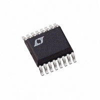
LTC1867LACGN#PBF Linear Technology, LTC1867LACGN#PBF Datasheet - Page 7

LTC1867LACGN#PBF
Manufacturer Part Number
LTC1867LACGN#PBF
Description
IC ADC 16BIT 8CH 175KSPS 16SSOP
Manufacturer
Linear Technology
Datasheet
1.LTC1863LCGNPBF.pdf
(16 pages)
Specifications of LTC1867LACGN#PBF
Number Of Bits
16
Sampling Rate (per Second)
175k
Data Interface
MICROWIRE™, Serial, SPI™
Number Of Converters
1
Power Dissipation (max)
2.7mW
Voltage Supply Source
Single Supply
Operating Temperature
0°C ~ 70°C
Mounting Type
Surface Mount
Package / Case
16-SSOP (0.150", 3.90mm Width)
Number Of Elements
1
Resolution
16Bit
Architecture
SAR
Sample Rate
175KSPS
Input Polarity
Unipolar/Bipolar
Input Type
Voltage
Rated Input Volt
2.5/±1.25V
Differential Input
Yes
Power Supply Requirement
Analog and Digital
Single Supply Voltage (typ)
3.3V
Single Supply Voltage (min)
2.7V
Single Supply Voltage (max)
3.6V
Dual Supply Voltage (typ)
Not RequiredV
Dual Supply Voltage (min)
Not RequiredV
Dual Supply Voltage (max)
Not RequiredV
Power Dissipation
2.7mW
Differential Linearity Error
-1LSB(Min)
Integral Nonlinearity Error
±3LSB
Operating Temp Range
0C to 70C
Operating Temperature Classification
Commercial
Mounting
Surface Mount
Pin Count
16
Package Type
SSOP N
Lead Free Status / RoHS Status
Lead free / RoHS Compliant
Available stocks
Company
Part Number
Manufacturer
Quantity
Price
PIN FUNCTIONS
TYPICAL PERFORMANCE CHARACTERISTICS
(LTC1863L/ LTC1867L)
CHO-CH7/COM (Pins 1-8): Analog Input Pins. Analog
inputs must be free of noise with respect to GND. CH7/COM
can be either a separate channel or the common minus
input for the other channels. Unused channels should be
tied to ground.
REFCOMP (Pin 9): Reference Buffer Output Pin. Bypass
to GND with 10μF tantalum capacitor in parallel with 0.1μF
ceramic capacitor (2.5V Nominal). To overdrive REFCOMP,
tie V
V
be used as an external reference buffer input for improved
accuracy and drift. Bypass to GND with 2.2μF tantalum
capacitor in parallel with 0.1μF ceramic capacitor.
CS/CONV (Pin 11): This input provides the dual function
of initiating conversions on the ADC and also frames the
serial data transfer.
REF
REF
(Pin 10): 1.25V Reference Output. This pin can also
to GND.
–0.25
–0.50
–0.75
–1.00
1.00
0.75
0.50
0.25
0
0
Integral Nonlinearity
vs Output Code (LTC1863L)
512
1024
1536
CODE
2048
2560
3072
3584
1863L7L G16
4096
SCK (Pin 12): Shift Clock. This clock synchronizes the
serial data transfer.
SDO (Pin 13): Digital Data Output. The A/D conversion
result is shifted out of this output. Straight binary format
for unipolar mode and two’s complement format for
bipolar mode.
SDI (Pin 14): Digital Data Input Pin. The A/D confi guration
word is shifted into this input.
GND (Pin 15): Analog and Digital GND.
V
GND with 10μF tantalum capacitor in parallel with 0.1μF
ceramic capacitor.
DD
(Pin 16): Analog and Digital Power Supply. Bypass to
–0.25
–0.50
–0.75
–1.00
1.00
0.75
0.50
0.25
0
0
Differential Nonlinearity
vs Output Code (LTC1863L)
512
1024
LTC1863L/LTC1867L
1536
2048
CODE
2560
3072
3584
1863L7L G17
4096
1863l7lfc
7


