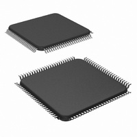
LM9830VJD/NOPB National Semiconductor, LM9830VJD/NOPB Datasheet - Page 6

LM9830VJD/NOPB
Manufacturer Part Number
LM9830VJD/NOPB
Description
IC SCANNER COLOR DOC 100-TQFP
Manufacturer
National Semiconductor
Datasheet
1.LM9830VJDNOPB.pdf
(45 pages)
Specifications of LM9830VJD/NOPB
Number Of Bits
12
Number Of Channels
3
Power (watts)
350mW
Voltage - Supply, Analog
5V
Voltage - Supply, Digital
4.5 V ~ 5.5 V
Package / Case
100-TQFP, 100-VQFP
Lead Free Status / RoHS Status
Lead free / RoHS Compliant
Other names
*LM9830VJD
*LM9830VJD/NOPB
LM9830VJD
*LM9830VJD/NOPB
LM9830VJD
Available stocks
Company
Part Number
Manufacturer
Quantity
Price
Company:
Part Number:
LM9830VJD/NOPB
Manufacturer:
Texas Instruments
Quantity:
10 000
Note 1: Absolute Maximum Ratings indicate limits beyond which damage to the device may occur. Operating Ratings indicate conditions for which the device is functional,
but do not guarantee specific performance limits. For guaranteed specifications and test conditions, see the Electrical Characteristics. The guaranteed specifications apply
only for the test conditions listed. Some performance characteristics may degrade when the device is not operated under the listed test conditions.
Note 2: All voltages are measured with respect to GND=AGND=DGND=DGND
Note 3: When the input voltage (V
imum package input current rating limits the number of pins that can simultaneously safely exceed the power supplies with an input current of 25mA to two.
Note 4: The maximum power dissipation must be derated at elevated temperatures and is dictated by T
able power dissipation at any temperature is P
is 53°C/W
Note 5: Human body model, 100pF capacitor discharged through a 1.5k resistor.
Note 6: See AN450 “Surface Mounting Methods and Their Effect on Product Reliability” or the section titled “Surface Mount” found in any National Semiconductor Linear
Data Book for other methods of soldering surface mount devices.
Note 7: Two diodes clamp the OS analog inputs to
impedance of the sensor, prevents damage to the LM9830 from transients during power-up.
Note 8: For best performance, it is required that all supply pins be powered from the same power supply with separate bypass capacitors at each supply pin.
Note 9: Typicals are at T
Note 10: Tested limits are guaranteed to National's AOQL (Average Outgoing Quality Level).
Note 11: Integral linearity error is defined as the deviation of the analog value, expressed in LSBs, from the straight line that best fits the actual transfer function of the ADC.
Note 12: V
a white (full scale) image with respect to the reference level, V
correctable range of pixel-to-pixel V
t
t
AC Electrical Characteristics
The following specifications apply for AGND=DGND=DGND
f
C
t
WR DATA SETUP
WR ADDR HOLD
CRYSTAL IN
WR DATA HOLD
t
t
L
WR R ADDR
t
WR F ADDR
Symbol
RD SETUP
(databus loading) = 20pF/pin. Boldface limits apply for T
SETUP
SETUP
.
t
SRAM Write Timing (Figure 8) - Typical Values Represent Worst Case Timing for Different MCLK Frequencies
WR
SRAM Read Timing (Figure 9) - Typical Values Represent Worst Case Timing for Different MCLK Frequencies
REF
is defined as the CCD OS voltage for the reference period following the reset feedthrough pulse. V
= 50MHz, MCLK DIVIDER = 1.0 (unless otherwise noted), f
Address valid to WR falling
Address valid to WR rising
DB0-DB7 valid to WR rising
WR rising to Address data change
Address valid to DB0-DB7 data valid
WR pulse width
WR rising to DB0-DB7 data Tri-State
J
=T
A
=25°C, f
IN
) at any pin exceeds the power supplies (V
WHITE
CRYSTAL IN
Parameter
variation is defined as the maximum variation in V
D
= (T
= 50MHz, and represent most likely parametric norm.
AGND
J
max - T
and
A
REF
) /
VA
OS Input
. V
JA
as shown below. This input protection, in combination with the external clamp capacitor and the output
RFT
. T
J
max = 150°C for this device. The typical thermal resistance (
is defined as the peak positive deviation above V
4 slot mode
8 slot mode
(f
MCLK
IN
I/O
I/O
<GND or V
AGND
=DGND
A
Conditions
=DGND
VA
= 25MHz)
=T
6
J
=T
SRAM
IN
MIN
>V
SRAM
To Internal
Circuitry
MCLK
WHITE
=0V, unless otherwise specified.
A
to T
or V
=0V, V
= f
MAX
D
(due to PRNU, light source intensity variation, optics, etc.) that the
), the current at that pin should be limited to 25mA. The 50mA max-
CRYSTAL IN
J
; all other limits T
max,
2 t
1 t
A
=V
0.33 t
0.5 t
1.5 t
MCLK
MCLK
(Note 9)
Typical
1 t
1 t
JA
D
WHITE
- 7ns
- 9ns
- 9ns
- 5ns
- 4ns
=V
MCLK
MCLK
and the ambient temperature, T
1
MCLK
MCLK
/MCLK DIVIDER, f
MCLK
- 12ns
- 12ns
DI/O
is defined as the peak CCD pixel output voltage for
REF
=V
of the reset feedthrough pulse. The maximum
SRAM
A
=T
(Note 10)
J
Limits
=25°C. (Notes 7 & 8)
=+5.0V
JA
21
11
15
28
3
2
4
) of this part when board mounted
ADC CLK
http://www.national.com
DC
,
A
. The maximum allow-
ns (max)
ns (max)
= f
(Limits)
ns (min)
ns (min)
ns (min)
ns (min)
ns (min)
Units
MCLK
/8,


