LM9830VJD/NOPB National Semiconductor, LM9830VJD/NOPB Datasheet
LM9830VJD/NOPB
Specifications of LM9830VJD/NOPB
*LM9830VJD/NOPB
LM9830VJD
Available stocks


Related parts for LM9830VJD/NOPB


LM9830VJD/NOPB Summary of contents
Page 1
... Ordering Information Commercial (0°C LM9830VJD LM9830VJDX TRI-STATE® registered trademark of National Semiconductor Corporation. ©1998 National Semiconductor Corporation scan resolution and pixel depth for maximum scan speed. • Stepper motor control tightly coupled with buffer management to maximize data transfer efficiency. • PWM stepper motor current control allows microstepping for the price of fullstepping. • ...
Page 2
Absolute Maximum Ratings + Positive Supply Voltage ( DI/O With Respect to GND=AGND=DGND=DGND =DGND I/O SRAM Voltage On Any Input or Output Pin Input Current at any pin (Note 3) Package Input Current (Note ...
Page 3
Electrical Characteristics (Continued) The following specifications apply for AGND=DGND=DGND f = 50MHz. Boldface limits apply for T CRYSTAL IN Symbol Parameter Static Offset DAC Characteristics (Configuration Registers 38, 39, and 3A) Monotonicity Offset DAC LSB size Offset DAC Adjustment Range ...
Page 4
DC and Logic Electrical Characteristics The following specifications apply for AGND=DGND=DGND f = 50MHz. Boldface limits apply for T CRYSTAL IN Symbol Parameter CRYSTAL IN, CRYSTAL OUT Characteristics XTAL CRYSTAL OUT Bias Level (Offset) OUT DC XTAL CRYSTAL OUT Amplitude ...
Page 5
AC Electrical Characteristics The following specifications apply for AGND=DGND=DGND f = 50MHz, MCLK DIVIDER = 1.0 (unless otherwise noted), f CRYSTAL IN C (databus loading) = 20pF/pin. Boldface limits apply for T L Symbol Parameter Parallel Port 8 Bit Data ...
Page 6
... Note 5: Human body model, 100pF capacitor discharged through a 1.5k resistor. Note 6: See AN450 “Surface Mounting Methods and Their Effect on Product Reliability” or the section titled “Surface Mount” found in any National Semiconductor Linear Data Book for other methods of soldering surface mount devices. ...
Page 7
LM9830 can correct for using its internal PGA. Note 13: PGA Gain Error is the maximum difference between the measured gain for any PGA code and the ideal gain calculated by using the formula V PGA code Gain --- - ...
Page 8
Timing Diagrams SETUP1 STROBE t SETUP2 SELECT IN AUTOFEED BUSY SETUP1 STROBE SELECT IN t SETUP2 AUTOFEED BUSY STROBE SELECT IN AUTOFEED BUSY ERROR (D0, D4) SELECT (D1, D5) ...
Page 9
Address ALE SETUP ALE (SELECTIN (INIT) WR (STROBE) RD (AUTOFEED) Figure 5: µP Mode Address Latch SETUP ALE (SELECTIN) CS (INIT) WR (STROBE) RD (AUTOFEED) Figure 6: µP Mode ...
Page 10
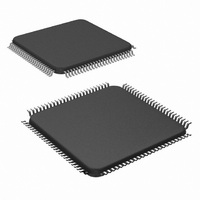
Connection Diagram 100 ...
Page 11
Pin Descriptions CCD Driver Signals ø1 Digital Output. CCD/CIS clock signal, phase 1. ø2 Digital Output. CCD clock signal, phase 2. RS Digital Output. Reset pulse for the CCD. CP1 Digital Output. Clamp pulse for the CCD. CP2 Digital Output. ...
Page 12
Digital Power Supplies V This is the positive supply pin for the D LM9830’s digital circuitry. It should be con- nected to a voltage source of +5V and bypassed to DGND with a 0.1µF monolithic capacitor. DGND This is the ...
Page 13
LM9830 Register Listing (Registers in bold boxes are reset to that value on power-up. All register addresses are in hexadecimal. All other numbers are decimal unless otherwise noted.) Address Function IMAGE BUFFER (READ ONLY) 00 Pixel (Image) Data STATUS REGISTERS ...
Page 14
Address Function COMMAND REGISTER Command Register This register is used to start and end a scan also used to home the sensor in a flatbed scanner or eject the image in a sheetfed scanner. 07 Standby When this ...
Page 15
Address Function RESERVED 0A Reserved SENSOR CONFIGURATION Input Signal Polarity CDS On/Off Standard/Even Odd Sensor 0B Sensor Resolution (used only for SRAM coefficient allocation) Line Skipping Color Phase Delay Part of the “n out of m” function, consisting of registers ...
Page 16
Address Function CIS TR1 Timing Mode 19 Fake Optical Black Pixels (for Dyna-type CIS sensors) RESERVED 1A Reserved Reserved 1B SENSOR PIXEL CONFIGURATION 1C Optical Black Pixels Start 1D Optical Black Pixels End 1E Active Pixels Start - MSB 1F ...
Page 17
Address Function COLOR MODE SETTINGS AFE Operation 3 Channel or 1 Channel 1 Channel Mode A Channel Color (1 Channel Mode B always uses the 26 Blue Channel) TR (=TR1) position RED (3 Channel Line Rate Mode only) TR (=TR2) ...
Page 18
Address Function ILLUMINATION SETTINGS Illumination Mode Controls the function of the 3 LAMP outputs, LAMP , LAMP , and LAMP Mode 0 is the Off/Reset state. 29 Mode 1 is typically used for CCFL lamps. Mode 2 ...
Page 19
Address Function DIGITAL PIXEL RATE OFFSET AND GAIN SETTINGS Multiplier Gain Range Smaller gain ranges provide finer control. Larger gain ranges correct for larger shading errors. 3E Offset/Gain data format Multiplier Coefficient Source Offset Coefficient Source 3F Fixed Offset Coefficient ...
Page 20
Address Function STEPPER MOTOR CONTROL SETTINGS 1 n (Line Skipping) 44 Part of the “n out of m” function, consisting of registers 0B (bits 4-7) 44, 45 (bit 5), and 5A. Full/Microstepping Current Sensing Phases = 0 for fullstepping = ...
Page 21
Address Function PAPER SENSOR SETTINGS Paper Sensor #1 Polarity Paper Sensor #1: Level/Edge sensitive Paper Sensor #1: Stop Scan 58 Paper Sensor #2 Polarity Paper Sensor #2: Level/Edge sensitive Paper Sensor #2: Stop Scan MISC I/O PIN SETTINGS Misc I/O ...
Page 22
Address Function TEST MODE SETTINGS 5B Reserved 5C ADC Output Code - MSB 5D ADC Output Code - LSB Reserved Offset Subtractor Input Select 5E CDS Signal 5F-6F Reserved 70 Parallel Port Noise Filter 71-7F Reserved ...
Page 23
Applications Information 1.0 THEORY OF OPERATION 1.1 Overview A scanner is composed of many different but tightly intercon- nected blocks (the analog front end and ADC, sensor clock gen- eration, stepper motor control, data buffering, parallel port I/O, and others). ...
Page 24
This equation also applies to the divide by 1.5 function. Divide DPI By (600 DPI sensor) (300 DPI sensor) 1 600 1.5 400 2 300 3 200 4 150 6 100 Figure 11: Decreasing Horizontal Resolution ...
Page 25
If there are not enough unpacked pixels at the end of a line to ...
Page 26
DAC, shown in Figure 17. Scan Mode DAC Voltage 0.5V for number of steps specified in Starting from Kickstart Steps register (0-7 dead stop register is 0 there is no kickstart current - movement begins ...
Page 27
Value Additional Lines to Store in SRAM 0 0(a only and (a, b and c) ... ... 7 7 Figure 22: Lines to Process after Pause Scan Signal Register When the Resume Scan signal ...
Page 28
Paused until a Resume Scan signal is received. During the hold current timeout period, the DAC output is held at 0.125V (the hold current) for FullStep mode, or the DAC outputs are held as they were prior to stopping ...
Page 29
Figure 29, and in slightly more detail in Figure 41. TR LAMP R LAMP G LAMP B Figure 29: Illumination Mode 2 Illumination Mode 3 is similar to Illumination Mode 2, except that the LAMP outputs ...
Page 30
RS pulse. This mode works for TR1 TR1 RS Trailing edge of End of Optical first RS pulse Figure 35: Fake Optical Black Pixels only, under all TR1 settings (normal and CIS TR1 Timing ...
Page 31
TR R LED G LED B LED COEF DATA SC = selected channel (=green in this example) Figure 40: 1 Channel Mode A • 1 Channel Mode B: This mode uses a sensor tied to the Blue ...
Page 32
To improve the performance of this mode, there is also a 12 bit/8 slot (full duplex) mode available. In this mode coefficient reads take 1 MCLK each (a total of 2 MCLKs). The high and low bytes of the ...
Page 33
Configuration Register Name Address DataPort 5 Address (LSB) 6 DataPort Figure 44: DataPort The DataPort allows the user to select a memory block (gamma, gain coefficient, or offset coefficient) and color (red, green, or blue read from or ...
Page 34
Additionally, the parallel port Name Direction Parallel Port Databus D0-D7 From (To Control Signals STROBE From PC AUTOFEED From PC INIT From PC SELECT IN From PC ACK To PC BUSY To ...
Page 35
STROBE SELECT IN AUTOFEED INIT Figure 51: LM9830 Transparent without Reset 6.5 Returning to Transparency Mode with LM9830 Reset The host can return the LM9830 to Transparency Mode and reset the LM9830 by taking the INIT, AUTOFEED, SELECT_IN, and ...
Page 36
ERROR (D0, D4) SELECT (D1, D5) D7-D4 PE (D2, D6) ACK (D3, D7) Addr STROBE SELECT IN AUTOFEED BUSY Figure 55: Reading from the Configuration Register (Nibble Mode) An EPP read is shown in Figure 55. The ...
Page 37
LM9830 in a continuous stream. First, write to register 3 to set what the data is (gamma or offset/gain) and what color (red, green, or blue) the data is for. Then write to registers 4 and 5 to ...
Page 38
,..., n-1 n-1 n-1 with the Red data representing line ...
Page 39
RD 48MHz 3 Overtone Crystal Ecliptek EC-T-48.000M 100 LM9830 CRYSTAL IN (57) 5pF 15pF 1.2µ 300pF Figure 63: Crystal Oscillator Circuit To use the LM9830’s crystal oscillator feature, tie ...
Page 40
The correct Default Phase Difference (registers 52 and 53) must be set for a scan to restart properly following a pause in the scan- ning. See the LM9830 software for information on setting the DPD register. Attempting to read out ...
Page 41
Digital Processing Block Diagram 8*f ADC (50MHz max) CRYSTAL OUT CRYSTAL IN System Clock Generation 8 Offset Latch Pixel-Rate 12-Bit Offset ADC Subtraction 10 bits CR Sensor (Offset and Gain) Address Counter Increment Buffer In Address Counter ...
Page 42
Analog Front End Block Diagram OS R RED OS from CCD OS G GREEN OS from CCD OS B BLUE OS from CCD V REF LO FORCE V REF LO SENSE V REF MID FORCE V REF MID SENSE V ...
Page 43
Stepper Motor Current Controller Block Diagram Phase A Invert DAC A: 0.125V, DAC code for 3 0.191V, phase A 0.353V, 0.462V, 0.500V CRYSTAL IN (50MHz) ÷ ÷1 to 256 ÷64 PWM 6 CR Generator 0/64 ...
Page 44
Printer Passthrough Block Diagram +5V from Scanner Power Supply 5 74HCT244 4 To Computer Control Signals Databus TRISTATE LM9830 Notes generated by rectifying the control outputs from the PC and printer parallel ports. If needed, ...
Page 45
... A critical component is any component of a life support device or system whose failure to perform can be reasonably expected to cause the failure of the life support device or system affect its safety or effectiveness. National Semiconductor Europe National Semiconductor Hong Kong Fax: a49 (0) 180-530 85 86 13th Floor, Straight Block, Email: europe.support @ nsc.com Ocean Centre, 5 Canton Rd ...