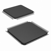
LM9830VJD/NOPB National Semiconductor, LM9830VJD/NOPB Datasheet - Page 4

LM9830VJD/NOPB
Manufacturer Part Number
LM9830VJD/NOPB
Description
IC SCANNER COLOR DOC 100-TQFP
Manufacturer
National Semiconductor
Datasheet
1.LM9830VJDNOPB.pdf
(45 pages)
Specifications of LM9830VJD/NOPB
Number Of Bits
12
Number Of Channels
3
Power (watts)
350mW
Voltage - Supply, Analog
5V
Voltage - Supply, Digital
4.5 V ~ 5.5 V
Package / Case
100-TQFP, 100-VQFP
Lead Free Status / RoHS Status
Lead free / RoHS Compliant
Other names
*LM9830VJD
*LM9830VJD/NOPB
LM9830VJD
*LM9830VJD/NOPB
LM9830VJD
Available stocks
Company
Part Number
Manufacturer
Quantity
Price
Company:
Part Number:
LM9830VJD/NOPB
Manufacturer:
Texas Instruments
Quantity:
10 000
DC and Logic Electrical Characteristics
The following specifications apply for AGND=DGND=DGND
f
CRYSTAL IN, CRYSTAL OUT Characteristics
Power Supply Characteristics
XTAL
XTAL
CRYSTAL IN
Symbol
AC Electrical Characteristics
The following specifications apply for AGND=DGND=DGND
f
C
CRYSTAL IN
I
L
D I/O
Symbol
t
t
t
t
I
(databus loading) = 20pF/pin. Boldface limits apply for T
SETUP1
SETUP2
t
t
SETUP1
SETUP2
t
t
OUT DC
A
t
t
t
OUT AC
HOLD1
HOLD2
HOLD1
HOLD2
t
t
AF-B1
B-AF1
AF-B2
t
SI-B1
SI-B2
B-SI
= 50MHz. Boldface limits apply for T
= 50MHz, MCLK DIVIDER = 1.0 (unless otherwise noted), f
CRYSTAL OUT Bias Level (Offset)
CRYSTAL OUT Amplitude
Analog Supply Current
(V
Digital I/O Supply Current
(V
A
D I/O
D0-D7 (Address) valid to SELECT IN
falling
STROBE falling edge to SELECT IN
falling
SELECT IN falling to BUSY rising
BUSY rising to SELECT IN rising
SELECT IN rising to STROBE rising
SELECT IN rising to BUSY falling
D0-D7 (Address) hold time after
BUSY falling
D0-D7 valid or STROBE falling to
SELECT IN falling
STROBE falling to AUTOFEED falling
AUTOFEED falling to BUSY rising
BUSY rising to AUTOFEED rising
AUTOFEED rising to STROBE rising
AUTOFEED rising to BUSY falling
D0-D7 valid after BUSY falling
pins)
, V
D
, and V
Parameter
Parameter
SRAM
pins)
Parallel Port Address Write (Figure 1)
Parallel Port Data Write (Figure 2)
A
=T
J
=T
MIN
All Except Dataport
Dataport
f
Operating
Standby
Operating
Standby
CRYSTAL
I/O
to T
I/O
=DGND
A
Conditions
MAX
=DGND
=T
4
= 50MHz
J
; all other limits T
=T
Conditions
SRAM
MIN
SRAM
MCLK
to T
=0V, V
=0V, V
= f
MAX
CRYSTAL IN
A
; all other limits T
=V
A
A
1.5 t
=V
=T
D
(Note 9)
=V
Typical
D
J
=25°C. (Notes 7 & 8)
=V
-60
-15
-45
-10
-60
-25
-40
ADC CLK
-10
25
33
34
16
DI/O
0
0
/MCLK DIVIDER, f
DI/O
=V
=V
(Note 9)
SRAM
Typical
0.75
SRAM
A
0.8
0.8
64
40
5
=T
3 t
(Note 10)
=+5.0V
J
=25°C. (Notes 7 & 8)
Limits
ADC CLK
=+5.0V
-10
-10
-15
-10
-10
-10
40
20
50
50
20
35
0
0
(Note 10)
DC
ADC CLK
Limits
http://www.national.com
0.95
,
DC
6.5
83
48
,
ns (max)
ns (max)
ns (max)
ns (max)
ns (max)
= f
(Limits)
ns (min)
ns (min)
ns (min)
ns (min)
ns (min)
ns (min)
ns (min)
ns (min)
ns (min)
ns (min)
Units
MCLK
mA (max)
mA (max)
mA (max)
mA (max)
(Limits)
Units
V
V
P-P
/8,


