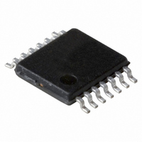
PCA2125TS/1,112 NXP Semiconductors, PCA2125TS/1,112 Datasheet - Page 3

PCA2125TS/1,112
Manufacturer Part Number
PCA2125TS/1,112
Description
IC CMOS RTC/CALENDAR 14-TSSOP
Manufacturer
NXP Semiconductors
Type
Clock/Calendar/Alarmr
Datasheet
1.PCA2125TS1112.pdf
(36 pages)
Specifications of PCA2125TS/1,112
Package / Case
14-TSSOP
Time Format
HH:MM:SS (12/24 hr)
Date Format
YY-MM-DD-dd
Interface
SPI, 3-Wire Serial
Voltage - Supply
1.3 V ~ 5.5 V
Operating Temperature
-40°C ~ 125°C
Mounting Type
Surface Mount
Function
Clock, Calendar
Supply Voltage (max)
5.5 V
Supply Voltage (min)
1.3 V
Maximum Operating Temperature
+ 125 C
Minimum Operating Temperature
- 40 C
Mounting Style
SMD/SMT
Rtc Bus Interface
Serial
Lead Free Status / RoHS Status
Lead free / RoHS Compliant
For Use With
OM6292 - DEMO BOARD PCA2125 RTC
Memory Size
-
Lead Free Status / RoHS Status
Lead free / RoHS Compliant, Lead free / RoHS Compliant
Other names
935283386112
PCA2125TS/1
PCA2125TS/1
PCA2125TS/1
PCA2125TS/1
NXP Semiconductors
7. Pinning information
8. Functional description
PCA2125_1
Product data sheet
7.1 Pinning
7.2 Pin description
Table 3.
The PCA2125 contains sixteen 8-bit registers with an auto-incrementing address register,
an on-chip 32.768 kHz oscillator with one integrated capacitor, a frequency divider which
provides the source clock for the Real-Time Clock (RTC), a programmable clock output,
and a 6 MHz SPI-bus.
All sixteen registers are designed as addressable 8-bit parallel registers although not all
bits are implemented:
Symbol
OSCI
OSCO
n.c.
INT
CE
V
SDO
SDI
SCL
n.c.
CLKOUT
V
Fig 2.
SS
DD
Pin configuration for TSSOP14
Pin description
Pin
1
2
3, 4
5
6
7
8
9
10
11, 12
13
14
Description
oscillator input
oscillator output
not connected; do not connect and do not use as feed through; connect
to V
interrupt output (open-drain; active LOW)
chip enable input (active HIGH) with 200 k pull-down resistor
ground
serial data output, push-pull
serial data input; might float when CE inactive
serial clock input; might float when CE inactive
not connected; do not connect and do not use as feed through; connect
to V
clock output (open-drain)
supply voltage
Rev. 01 — 28 July 2008
OSCO
DD
DD
OSCI
V
n.c.
n.c.
INT
CE
SS
if floating pins are not allowed
if floating pins are not allowed
1
2
3
4
5
6
7
PCA2125
001aaf892
14
13
12
11
10
9
8
V
CLKOUT
n.c.
n.c.
SCL
SDI
SDO
DD
SPI Real-time clock/calendar
PCA2125
© NXP B.V. 2008. All rights reserved.
3 of 36


