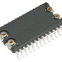
M48T201Y-70MH1E STMicroelectronics, M48T201Y-70MH1E Datasheet - Page 15

M48T201Y-70MH1E
Manufacturer Part Number
M48T201Y-70MH1E
Description
IC SUPERVISOR TIMEKPR 5V 44-SOH
Manufacturer
STMicroelectronics
Series
Timekeeper®r
Type
Clock/Calendar/NVSRAMr
Datasheet
1.M48T201V-85MH1F.pdf
(37 pages)
Specifications of M48T201Y-70MH1E
Memory Size
External
Time Format
HH:MM:SS (24 hr)
Date Format
YY-MM-DD-dd
Interface
Parallel
Voltage - Supply
4.5 V ~ 5.5 V
Operating Temperature
0°C ~ 70°C
Mounting Type
Surface Mount
Package / Case
44-SOH
Number Of Voltages Monitored
1
Monitored Voltage
3.3 V, 5 V
Manual Reset
Not Resettable
Watchdog
Watchdog
Battery Backup Switching
Backup
Supply Voltage (max)
5.5 V
Supply Voltage (min)
4.5 V
Supply Current (typ)
15000 uA
Maximum Power Dissipation
1000 mW
Maximum Operating Temperature
+ 70 C
Mounting Style
SMD/SMT
Minimum Operating Temperature
0 C
Power Fail Detection
Yes
Lead Free Status / RoHS Status
Contains lead / RoHS non-compliant
Other names
497-2840-5
M48T201Y-70MH1
M48T201Y-70MH1
M48T201Y, M48T201V
2.4
Table 4.
1. Valid for ambient operating temperature: T
2. C
3. If E goes low simultaneously with W going low, the outputs remain in the high impedance state.
Data retention mode
With valid V
or WRITE cycles. Should the supply voltage decay, the M48T201Y/V will automatically
deselect, write protecting itself (and any external SRAM) when V
(max) and V
registers via the E signal. At this time, the reset pin (RST) is driven active and will remain
active until V
manner by forcing E
remain at this level as long as V
below the level of the battery (V
SNAPHAT
External RAM is also powered by the SNAPHAT battery. All outputs except G
RST, IRQ/FT and V
100 µA of current to the attached memory with less than 0.3 V drop under this condition. On
power up, when V
by inhibiting E
page
t
t
WHQX
WLQZ
Symbol
t
t
t
t
t
t
t
noted).
t
t
t
t
t
t
WLWH
WHDX
WHAX
DVWH
AVWH
AVWL
EHAX
EHDX
ELEH
DVEH
AVEH
AVAV
AVEL
L
30).
= 5 pF
(2)(3)
(2)(3)
®
CC
WRITE cycle time
Address valid to WRITE enable low
Address valid to chip enable low
WRITE enable pulse width
Chip enable low to chip enable high
WRITE enable high to address transition
Chip enable high to address transition
Input valid to WRITE enable high
Input valid to chip enable high
WRITE enable high to input transition
Chip enable high to input transition
WRITE enable low to output High-Z
Address valid to WRITE enable high
Address valid to chip enable high
WRITE enable high to output transition
PFD
battery and the clock registers are maintained from the attached battery supply.
CC
Write mode AC characteristics
CON
applied, the M48T201Y/V can be accessed as described above with READ
returns to nominal levels. External RAM access is inhibited in a similar
(min). This is accomplished by internally inhibiting access to the clock
CC
. The RST signal also remains active during this time (see
OUT
CON
returns to a nominal value, write protection continues for 200 ms (max)
, become high impedance. The V
to a high level. This level is within 0.2 V of the V
Parameter
CC
BAT
remains at an out-of-tolerance condition. When V
), power input is switched from the V
(1)
A
= 0 to 70°C; V
CC
= 4.5 to 5.5 V or 3.0 to 3.6 V (except where
Min
M48T201Y
70
45
50
25
25
55
55
0
0
0
0
0
0
5
OUT
–70
pin is capable of supplying
Max
20
CC
falls between V
Min
85
55
60
30
30
65
65
M48T201V
0
0
0
0
0
0
5
CC
BAT
–85
pin to the
. E
Figure 14 on
CON
Max
CON
25
Operation
, E
will
PFD
CC
CON
Unit
15/37
ns
ns
ns
ns
ns
ns
ns
ns
ns
ns
ns
ns
ns
ns
ns
falls
,


