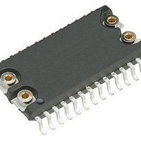
M48T201Y-70MH1E STMicroelectronics, M48T201Y-70MH1E Datasheet - Page 13

M48T201Y-70MH1E
Manufacturer Part Number
M48T201Y-70MH1E
Description
IC SUPERVISOR TIMEKPR 5V 44-SOH
Manufacturer
STMicroelectronics
Series
Timekeeper®r
Type
Clock/Calendar/NVSRAMr
Datasheet
1.M48T201V-85MH1F.pdf
(37 pages)
Specifications of M48T201Y-70MH1E
Memory Size
External
Time Format
HH:MM:SS (24 hr)
Date Format
YY-MM-DD-dd
Interface
Parallel
Voltage - Supply
4.5 V ~ 5.5 V
Operating Temperature
0°C ~ 70°C
Mounting Type
Surface Mount
Package / Case
44-SOH
Number Of Voltages Monitored
1
Monitored Voltage
3.3 V, 5 V
Manual Reset
Not Resettable
Watchdog
Watchdog
Battery Backup Switching
Backup
Supply Voltage (max)
5.5 V
Supply Voltage (min)
4.5 V
Supply Current (typ)
15000 uA
Maximum Power Dissipation
1000 mW
Maximum Operating Temperature
+ 70 C
Mounting Style
SMD/SMT
Minimum Operating Temperature
0 C
Power Fail Detection
Yes
Lead Free Status / RoHS Status
Contains lead / RoHS non-compliant
Other names
497-2840-5
M48T201Y-70MH1
M48T201Y-70MH1
M48T201Y, M48T201V
2.3
Table 3.
1. Valid for ambient operating temperature: T
2. C
Write mode
The M48T201Y/V is in the WRITE mode whenever W (WRITE enable) and E (chip enable)
are low state after the address inputs are stable. The start of a WRITE is referenced from
the latter occurring falling edge of W or E. A WRITE is terminated by the earlier rising edge
of W or E. The addresses must be held valid throughout the cycle. E or W must return high
for a minimum of t
of another READ or WRITE cycle. Data-in must be valid t
and remain valid for t
bus contention; although, if the output bus has been activated by a low on E and G a low on
W will disable the outputs t
When the address value presented to the M48T201Y/V during the WRITE is in the range of
7FFFFh-7FFF0h, one of the on-board TIMEKEEPER
will be written into the device. When the address value presented to M48T201Y/V is outside
the range of TIMEKEEPER registers, an external SRAM location is selected.
Symbol
t
t
t
t
GHQZ
ELQX
GLQX
EHQZ
t
t
t
t
t
t
t
t
AVQV
GLQV
AXQX
AOEH
t
OERL
ELQV
AOEL
AVAV
noted).
t
EPD
RO
L
= 5 pF.
(2)
(2)
(2)
(2)
READ cycle time
Address valid to output valid
Chip enable low to output valid
Output enable low to output valid
Chip enable low to output transition
Output enable low to output transition
Chip enable high to output Hi-Z
Output enable high to output Hi-Z
Address transition to output transition
External SRAM address to G
Supervisor SRAM address to G
E to E
G low to G
G high to G
Read mode AC characteristics
CON
EHAX
CON
low or high
CON
WHDX
from chip enable or t
low
Parameter
high
WLQZ
afterward. G should be kept high during WRITE cycles to avoid
after W falls.
(1)
CON
A
= 0 to 70°C; V
CON
low
high
WHAX
CC
from WRITE enable prior to the initiation
= 4.5 to 5.5 V or 3.0 to 3.6 V (except where
®
Min
70
M48T201Y
registers will be selected and data
5
0
5
DVWH
–70
Max
20
70
70
25
20
20
20
10
15
10
prior to the end of WRITE
Min
M48T201V
85
5
0
5
–85
Max
85
85
35
25
25
30
30
15
20
15
Operation
Unit
ns
ns
ns
ns
ns
ns
ns
ns
ns
ns
ns
ns
ns
ns
13/37


