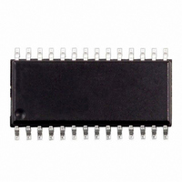
M41ST87WMX6TR STMicroelectronics, M41ST87WMX6TR Datasheet - Page 21

M41ST87WMX6TR
Manufacturer Part Number
M41ST87WMX6TR
Description
IC SUPERVISOR RTC 160X8 28-SOIC
Manufacturer
STMicroelectronics
Type
Clock/Calendar/Supervisorr
Specifications of M41ST87WMX6TR
Memory Size
160B
Time Format
HH:MM:SS:hh (24 hr)
Date Format
YY-MM-DD-dd
Interface
I²C, 2-Wire Serial
Voltage - Supply
2.7 V ~ 3.6 V
Operating Temperature
-40°C ~ 85°C
Mounting Type
Surface Mount
Package / Case
28-SOIC, 28-SOH (8.48mm Width)
Bus Type
Serial (2-Wire, I2C)
Operating Supply Voltage (typ)
3.3V
Operating Supply Voltage (max)
3.6V
Operating Supply Voltage (min)
2.7V
Operating Temperature Classification
Industrial
Operating Temperature (max)
85C
Operating Temperature (min)
-40C
Pin Count
28
Mounting
Surface Mount
Lead Free Status / RoHS Status
Lead free / RoHS Compliant
Other names
497-6457-2
M41ST87WMX6TR
M41ST87WMX6TR
Available stocks
Company
Part Number
Manufacturer
Quantity
Price
Company:
Part Number:
M41ST87WMX6TR
Manufacturer:
MBI
Quantity:
12 000
M41ST87Y, M41ST87W
2.6.6
Note:
2.6.7
2.6.8
2.6.9
Note:
Note:
Tamper detect sampling (TDS1 and TDS2)
This bit selects between a 1Hz sampling rate or constant monitoring of the tamper input
pin(s) to detect a tamper event when the normally closed switch mode is selected. This
allows the user to reduce the current drain when the TEB
in battery backup (see
if the TCM
“Don’t care.”
The crystal oscillator must be “on” for sampling to be enabled.
Tamper current high/tamper current low (TCHI/TCLO1 and
TCHI/TCLO2)
This bit selects the strength of the internal pull-up or pull-down used during the sampling of
the normally closed condition. The state of the TCHI/TCLO
open (TCM
RAM clear (CLR1 and CLR2)
When either of these bits and the TEB
user RAM (see
condition. The 128 bytes of user RAM will be deselected (invalid data will be read) until the
corresponding TEB
RAM clear external (CLR1
When either of these bits are set to a logic '1' and the TEB
external SRAM will be cleared and the RST output enabled (see
Figure 19 on page
The reset output resulting from a tamper event will be the same as a reset resulting from a
power-down condition, a watchdog time-out, or a manual reset (RSTIN1 or RSTIN2).
This is accomplished by forcing TP
regulator (see
of power to the V
tamper occurs during battery back-up (see
regulator, the user will also prevent other inputs from sourcing current to the external SRAM,
allowing it to retain data.
The user may optionally connect an inverting charge pump to the V
SRAM (see
manufacturing of the external SRAM, clearing the memory may require varying durations of
negative potential on the V
the time needed for their particular application. Control Bits CLRPW0 and CLRPW1
determine the duration TP
page
When using the inverting charge pump, the user must also provide isolation in the form of
two additional small-signal power MOSFETs. These will isolate the V
negative voltage generated by the charge pump during a tamper condition, and from being
pulled to ground by the output of the charge pump when it is in shut-down mode (SHDN =
logic low). The gates of both MOSFETs should be connected to TP
Figure 19 on page
24).
X
X
bit is set to logic '1' (Normally Open). In this case the state of the TDS
Figure 19 on page
= '1') mode (see
Figure 19 on page
Figure 14 on page
CC
24).
24. One n-channel enhancement MOSFET should be placed between
X
pin. V
bit is reset to '0.'
Table 4 on page 22
OUT
CLR
CC
Figure 17 on page
pin. This device configuration will allow the user to program
will automatically be disconnected from the battery if the
will be enabled (see
24). Depending on the process technology used for the
EXT
24) will also switch off V
CLR
20) will be cleared to all zeros in the event of a tamper
and CLR2
X
high, which if used to control the inhibit pin of the DC
bit are set to a logic '1,' the internal 128 bytes of
and
Figure 18 on page
Figure 16 on page
23).
EXT
Figure 18 on page 23
)
X
OUT
X
X
bit is enabled while the device is
bit is a “Don’t care” for normally
bit is also set to logic '1,' the
, depriving the external SRAM
23). By inhibiting the DC
Figure 14 on page 20
22). Sampling is disabled
CC
CLR
OUT
pin of the external
as shown in
Operating modes
pin from both the
and
Table 5 on
X
bit is a
21/48
and


