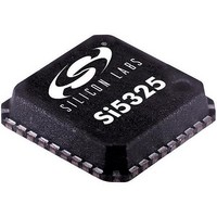
SI5325C-B-GM Silicon Laboratories Inc, SI5325C-B-GM Datasheet - Page 2

SI5325C-B-GM
Manufacturer Part Number
SI5325C-B-GM
Description
IC UP-PROG CLK MULTIPLIER 36QFN
Manufacturer
Silicon Laboratories Inc
Type
Clock Multiplierr
Specifications of SI5325C-B-GM
Number Of Circuits
1
Package / Case
36-QFN
Pll
Yes
Input
Clock
Output
CML, CMOS, LVDS, LVPECL
Ratio - Input:output
2:2
Differential - Input:output
Yes/Yes
Frequency - Max
346MHz
Divider/multiplier
Yes/Yes
Voltage - Supply
1.62 V ~ 3.63 V
Operating Temperature
-40°C ~ 85°C
Mounting Type
Surface Mount
Frequency-max
346MHz
Maximum Input Frequency
710 MHz
Minimum Input Frequency
10 MHz
Output Frequency Range
10 MHz to 1417 MHz
Supply Voltage (max)
3.63 V
Supply Voltage (min)
1.62 V
Maximum Operating Temperature
+ 85 C
Minimum Operating Temperature
- 40 C
Mounting Style
SMD/SMT
Operating Supply Voltage
1.8 V, 2.5 V, 3.3 V
Lead Free Status / RoHS Status
Lead free / RoHS Compliant
Si5325
Table 1. Performance Specifications
(V
2
Temperature Range
Supply Voltage
Supply Current
Input Clock Frequency
(CKIN1, CKIN2)
Output Clock Frequency
(CKOUT1, CKOUT2)
Input Clocks (CKIN1, CKIN2)
Differential Voltage Swing
Common Mode Voltage
Rise/Fall Time
Output Clocks (CKOUT1, CKOUT2)
Common Mode
Differential Output Swing
Single Ended Output
Swing
Note: For a more comprehensive listing of device specifications, please consult the Silicon Laboratories Any-Rate Precision
Duty Cycle
DD
= 1.8, 2.5, or 3.3 V ±10%, T
Clock Family Reference Manual. This document can be downloaded from www.silabs.com/timing.
Parameter
CKN
CKN
CKN
Symbol
CKN
A
CK
V
CK
V
V
= –40 to 85 ºC)
V
I
OCM
T
DD
DD
OD
SE
A
OF
VCM
DPP
TRF
F
DC
device PLL dividers. Consult
Silicon Laboratories configu-
ration software DSPLLsim at
quency/clock multiplication
determine PLL divider set-
tings for a given input fre-
Input frequency and clock
www.silabs.com/timing
multiplication ratio deter-
mined by programming
Both CKOUTs enabled
Both CKOUTs enabled
LVPECL format output
CMOS format output
Tristate/Sleep Mode
f
CKOUT2 disabled
CKOUT2 disabled
OUT
f
ratio combination.
Whichever is less
OUT
Test Condition
Preliminary Rev. 0.26
1.8 V ±10%
2.5 V ±10%
3.3 V ±10%
100 Ω load
line-to-line
= 622.08 MHz
LVPECL
20–80%
= 19.44 MHz
to
V
DD
1213
2.97
2.25
1.62
0.25
Min
–40
970
0.9
1.0
1.1
1.1
0.5
—
—
—
—
—
10
10
40
50
– 1.42
TBD
Typ
251
217
204
194
3.3
2.5
1.8
25
—
—
—
—
—
—
—
—
—
—
—
—
—
—
V
DD
1134
1417
TBD
Max
3.63
2.75
1.98
1.95
0.93
279
243
234
220
710
945
1.9
1.4
1.7
1.9
85
11
60
—
– 1.25
MHz
MHz
Unit
V
mA
mA
mA
mA
mA
ºC
ns
ns
%
V
V
V
V
V
V
V
V
V
PP


