SI5325C-B-GM Silicon Laboratories Inc, SI5325C-B-GM Datasheet
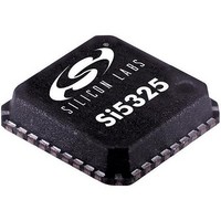
IC UP-PROG CLK MULTIPLIER 36QFN

SI5325C-B-GM

Manufacturer Part Number
SI5325C-B-GM
Description
IC UP-PROG CLK MULTIPLIER 36QFN
Manufacturer
Silicon Laboratories Inc
Type
Clock Multiplierr
Datasheets

Specifications of SI5325C-B-GM

Number Of Circuits
1
Package / Case
36-QFN
Pll
Yes
Input
Clock
Output
CML, CMOS, LVDS, LVPECL
Ratio - Input:output
2:2
Differential - Input:output
Yes/Yes
Frequency - Max
346MHz
Divider/multiplier
Yes/Yes
Voltage - Supply
1.62 V ~ 3.63 V
Operating Temperature
-40°C ~ 85°C
Mounting Type
Surface Mount
Frequency-max
346MHz
Maximum Input Frequency
710 MHz
Minimum Input Frequency
10 MHz
Output Frequency Range
10 MHz to 1417 MHz
Supply Voltage (max)
3.63 V
Supply Voltage (min)
1.62 V
Maximum Operating Temperature
+ 85 C
Minimum Operating Temperature
- 40 C
Mounting Style
SMD/SMT
Operating Supply Voltage
1.8 V, 2.5 V, 3.3 V
Lead Free Status / RoHS Status
Lead free / RoHS Compliant
µP-P
Description
The Si5325 is a low jitter, precision clock multiplier for
applications requiring clock multiplication without jitter
attenuation. The Si5325 accepts dual clock inputs ranging
from 10 to 710 MHz and generates two clock outputs ranging
from 10 to 945 MHz and select frequencies to 1.4 GHz. The
two outputs are divided down separately from a common
source. The device provides virtually any frequency
translation combination across this operating range. The
Si5325 input clock frequency and clock multiplication ratio
are programmable through an I
Si5325 is based on Silicon Laboratories' 3rd-generation
DSPLL
synthesis in a highly integrated PLL solution that eliminates
the need for external VCXO and loop filter components. The
DSPLL loop bandwidth is digitally programmable, providing
jitter performance optimization at the application level.
Operating from a single 1.8, 2.5, or 3.3 V supply, the Si5325
is ideal for providing clock multiplication in high performance
timing applications
Applications
Preliminary Rev. 0.26 7/07
Alarms
CKIN1
CKIN2
SONET/SDH OC-48/OC-192 line cards
GbE/10GbE, 1/2/4/8/10GFC line cards
ITU G.709 and custom FEC line cards
Optical modules
Wireless basestations
Data converter clocking
xDSL
SONET/SDH + PDH clock synthesis
Test and measurement
This information applies to a product under development. Its characteristics and specifications are subject to change without notice.
®
technology, which provides any-rate frequency
R O G R A M M A B L E
.
÷ N32
÷ N31
Signal Detect
2
C or SPI interface. The
Device Interrupt
Copyright © 2007 by Silicon Laboratories
I
2
C/SPI Port
P
R E C I S I O N
DSPLL
Control
÷ N2
®
Features
Clock Select
Generates any frequency from 10 to 945 MHz and
select frequencies to 1.4 GHz from an input
frequency of 10 to 710 MHz
Low jitter clock outputs w/jitter generation as low as
0.6 ps rms (30 kHz–1.3 MHz)
Integrated loop filter with selectable loop bandwidth
(150 kHz to 2 MHz)
Dual clock inputs w/manual or automatically
controlled hitless switching
Dual clock outputs with selectable signal format
(LVPECL, LVDS, CML, CMOS)
Support for ITU G.709 and custom FEC ratios
(255/238, 255/237, 255/236)
LOS, FOS alarm outputs
Digitally-controlled output phase adjust
I
On-chip voltage regulator for 1.8, 2.5, or 3.3 V
±10% operation
Small size: 6 x 6 mm 36-lead QFN
Pb-free, ROHS compliant
2
C or SPI programmable
C
L O C K
÷ NC2
÷ NC1
P
R E L I M I N A R Y
M
U L T I P L I E R
Si5325
D
VDD (1.8, 2.5, or 3.3 V)
GND
CKOUT1
CKOUT2
A TA
S
H E E T
Si5325

Related parts for SI5325C-B-GM

SI5325C-B-GM Summary of contents

Page 1

Description The Si5325 is a low jitter, precision clock multiplier for applications requiring clock multiplication without jitter attenuation. The Si5325 accepts dual clock inputs ranging from 10 to ...

Page 2

Si5325 Table 1. Performance Specifications (V = 1.8, 2.5, or 3.3 V ±10 – º Parameter Symbol Temperature Range T A Supply Voltage V DD Supply Current I DD Input Clock Frequency CK F ...

Page 3

Table 1. Performance Specifications (Continued 1.8, 2.5, or 3.3 V ±10 – º Parameter Symbol Rise/Fall Time CKO TRF Duty Cycle CKO DC PLL Performance Jitter Generation J GEN Jitter Transfer J ...

Page 4

Si5325 130 Ω 82 Ω Input Clock Sources* 130 Ω 82 Ω Control Mode (L) Reset Figure 1. Si5325 Typical Application Circuit (I2C Control Mode 3 ...

Page 5

Functional Description The Si5325 is a low jitter, precision clock multiplier for applications requiring clock multiplication without jitter attenuation. The Si5325 accepts dual clock inputs ranging from 10 to 710 MHz and generates two independent, synchronous clock outputs ranging ...

Page 6

Si5325 2. Pin Descriptions: Si5325 INT_C1B VDD GND GND Pin numbers are preliminary and subject to change. Pin # Pin Name I RST 14, NC — 18, 19, 20, 30 INT_C1B O Note: ...

Page 7

Table 3. Si5325 Pin Descriptions (Continued) Pin # Pin Name I/O 4 C2B O 5, 10 GND GND 12 CKIN2 CKIN2– 16 CKIN1 CKIN1– 21 CS_CA ...

Page 8

Si5325 Table 3. Si5325 Pin Descriptions (Continued) Pin # Pin Name I/O 22 SCL I 23 SDA_SDO I A2_SS I 27 SDI I 29 CKOUT1– CKOUT1+ 34 CKOUT2– CKOUT2+ 36 ...

Page 9

... Ordering Guide Ordering Part Output Clock Frequency Number Si5325A-B-GM 970–1134 MHz 1.213–1.417 GHz Si5325B-B-GM Si5325C-B-GM Package Range 10–945 MHz 36-Lead QFN 10–808 MHz 36-Lead QFN 10–346 MHz 36-Lead QFN Preliminary Rev. 0.26 Si5325 Temperature Range – °C – °C – ...

Page 10

Si5325 4. Package Outline: 36-Pin QFN Figure 3 illustrates the package details for the Si5325. Table 4 lists the values for the dimensions shown in the illustration. Figure 3. 36-Pin Quad Flat No-lead (QFN) Symbol Millimeters Min Nom A 0.80 ...

Page 11

Recommended PCB Layout Figure 4. PCB Land Pattern Diagram Preliminary Rev. 0.26 Si5325 11 ...

Page 12

Si5325 Table 5. PCB Land Pattern Dimensions Dimension Notes (General): 1. All dimensions shown are in millimeters (mm) unless otherwise noted. 2. Dimensioning and Tolerancing is per the ANSI ...

Page 13

OCUMENT HANGE IST Revision 0.23 to Revision 0.24 Clarified that the two outputs have a common, higher frequency source on page 1. Changed LVTTL to LVCMOS in Table 2, “Absolute Maximum Ratings,” on page 3. Added Figure ...

Page 14

... Should Buyer purchase or use Silicon Laboratories products for any such unintended or unauthorized ap- plication, Buyer shall indemnify and hold Silicon Laboratories harmless against all claims and damages. Silicon Laboratories, Silicon Labs, and DSPLL are trademarks of Silicon Laboratories Inc. Other products or brandnames mentioned herein are trademarks or registered trademarks of their respective holders. ...

Related keywords