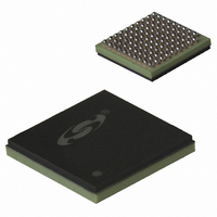
SI5364-G-BC Silicon Laboratories Inc, SI5364-G-BC Datasheet - Page 31

SI5364-G-BC
Manufacturer Part Number
SI5364-G-BC
Description
IC PREC PORT CARD CLOCK 99CBGA
Manufacturer
Silicon Laboratories Inc
Type
Clock Generatorr
Datasheet
1.SI5364-H-GL.pdf
(38 pages)
Specifications of SI5364-G-BC
Package / Case
99-CBGA
Pll
Yes
Input
Clock
Output
CML
Number Of Circuits
1
Ratio - Input:output
3:4
Differential - Input:output
Yes/Yes
Frequency - Max
675MHz
Divider/multiplier
No/Yes
Voltage - Supply
3.135 V ~ 3.465 V
Operating Temperature
-20°C ~ 85°C
Mounting Type
Surface Mount
Frequency-max
675MHz
Mounting Style
SMD/SMT
Operating Supply Voltage
2.3 V to 3.3 V
Lead Free Status / RoHS Status
Contains lead / RoHS non-compliant
Other names
336-1280
Available stocks
Company
Part Number
Manufacturer
Quantity
Price
Company:
Part Number:
SI5364-G-BC
Manufacturer:
LATTICE
Quantity:
190
Company:
Part Number:
SI5364-G-BC
Manufacturer:
SILICON
Quantity:
748
Company:
Part Number:
SI5364-G-BC
Manufacturer:
Silicon Laboratories Inc
Quantity:
10 000
Part Number:
SI5364-G-BC
Manufacturer:
SILICON LABS/芯科
Quantity:
20 000
*Note: The LVTTL inputs on the Si5364 device have an internal pulldown mechanism that causes the input to default to a logic
E7–9, F7–9,
F3, G3, H3–
E4–6, F4–6
G4–8, H8,
D4–9, E3,
7, J5, K5
J8, K8
Pin #
D3
K1
J2
low state if the input is not driven from an external source.
Pin Name
VALTIME
VSEL33
V
V
REXT
GND
DD33
DD25
Table 10. Pin Descriptions (Continued)
GND
V
V
I/O
I*
I*
I*
DD
DD
Signal Level
Analog
Supply
Supply
Supply
LVTTL
LVTTL
Rev. 2.5
Clock Validation Time for LOS and FOS.
VALTIME sets the clock validation times for recovery
from an LOS or FOS alarm condition. When VAL-
TIME is high, the validation time is approximately
13 s. When VALTIME is low, the validation time is
approximately 100 ms .
Select 3.3 V V
This is an enable pin for the internal regulator. To
enable the regulator, connect this pin to the V
pins.
3.3 V Supply.
3.3 V power is applied to the V
supply bypassing/decoupling for this configuration is
indicated in the typical application diagram for 3.3 V
supply operation.
2.5 V Supply.
These pins provide a means of connecting the
compensation network for the on-chip regulator.
Ground.
Must be connected to system ground. Minimize the
ground path impedance for optimal performance of
the device.
External Biasing Resistor.
Establishes bias currents within the device. This pin
must be connected to GND through a 10 k Ω (1%)
resistor.
DD
Supply.
Description
DD33
pins. Typical
Si5364
DD33
31


