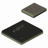
SI5364-G-BC Silicon Laboratories Inc, SI5364-G-BC Datasheet - Page 24

SI5364-G-BC
Manufacturer Part Number
SI5364-G-BC
Description
IC PREC PORT CARD CLOCK 99CBGA
Manufacturer
Silicon Laboratories Inc
Type
Clock Generatorr
Datasheet
1.SI5364-H-GL.pdf
(38 pages)
Specifications of SI5364-G-BC
Package / Case
99-CBGA
Pll
Yes
Input
Clock
Output
CML
Number Of Circuits
1
Ratio - Input:output
3:4
Differential - Input:output
Yes/Yes
Frequency - Max
675MHz
Divider/multiplier
No/Yes
Voltage - Supply
3.135 V ~ 3.465 V
Operating Temperature
-20°C ~ 85°C
Mounting Type
Surface Mount
Frequency-max
675MHz
Mounting Style
SMD/SMT
Operating Supply Voltage
2.3 V to 3.3 V
Lead Free Status / RoHS Status
Contains lead / RoHS non-compliant
Other names
336-1280
Available stocks
Company
Part Number
Manufacturer
Quantity
Price
Company:
Part Number:
SI5364-G-BC
Manufacturer:
LATTICE
Quantity:
190
Company:
Part Number:
SI5364-G-BC
Manufacturer:
SILICON
Quantity:
748
Company:
Part Number:
SI5364-G-BC
Manufacturer:
Silicon Laboratories Inc
Quantity:
10 000
Part Number:
SI5364-G-BC
Manufacturer:
SILICON LABS/芯科
Quantity:
20 000
Si5364
24
*Note: The LVTTL inputs on the Si5364 device have an internal pulldown mechanism that causes the input to default to a logic
Pin #
C2
C1
G1
G2
low state if the input is not driven from an external source.
CLKIN_A+
CLKIN_A–
CLKIN_B+
CLKIN_B–
Pin Name
I/O
I*
I*
Table 10. Pin Descriptions
200–500 mV
200–500 mV
(See Table 2)
(See Table 2)
Signal Level
AC Coupled
AC Coupled
Rev. 2.5
PPD
PPD
System Clock Input A.
One of three differential clock inputs selected by the
DSPLL when generating the SONET/SDH compliant
clock outputs. The frequencies of the Si5364 clock
outputs are each a 1, 8, or 32x multiple of the fre-
quency of the selected clock input. The multiplication
ratio is selected using Frequency Select (FRQSEL)
control pins associated with each clock output. An
additional scaling factor of either 238/255 or 255/238
is selected for FEC operation using the FEC[1:0]
control pins.
The clock input frequency is nominally 19.44 MHz.
The clock input frequency can be varied over the
range indicated in Table 3 on page 8 to produce
other output frequencies.
CLKIN_A is the highest priority clock input during
automatic switching mode operation.
System Clock Input B.
One of three differential clock inputs selected by the
DSPLL when generating the SONET/SDH compliant
clock outputs. The frequencies of the Si5364 clock
outputs are each a 1, 8, or 32x multiple of the fre-
quency of the selected clock input. The multiplication
ratio is selected using Frequency Select (FRQSEL)
control pins associated with each clock output. An
additional scaling factor of either 238/255 or 255/238
can be selected for FEC operation using the
FEC[1:0] control pins.
The clock input frequency is nominally 19.44 MHz.
and can be varied over the range indicated in Table 3
on page 8 to produce other output frequencies.
CLKIN_B is the second highest priority clock input
during automatic switching mode operation.
Description


