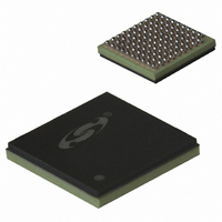
SI5364-G-BC Silicon Laboratories Inc, SI5364-G-BC Datasheet - Page 18

SI5364-G-BC
Manufacturer Part Number
SI5364-G-BC
Description
IC PREC PORT CARD CLOCK 99CBGA
Manufacturer
Silicon Laboratories Inc
Type
Clock Generatorr
Datasheet
1.SI5364-H-GL.pdf
(38 pages)
Specifications of SI5364-G-BC
Package / Case
99-CBGA
Pll
Yes
Input
Clock
Output
CML
Number Of Circuits
1
Ratio - Input:output
3:4
Differential - Input:output
Yes/Yes
Frequency - Max
675MHz
Divider/multiplier
No/Yes
Voltage - Supply
3.135 V ~ 3.465 V
Operating Temperature
-20°C ~ 85°C
Mounting Type
Surface Mount
Frequency-max
675MHz
Mounting Style
SMD/SMT
Operating Supply Voltage
2.3 V to 3.3 V
Lead Free Status / RoHS Status
Contains lead / RoHS non-compliant
Other names
336-1280
Available stocks
Company
Part Number
Manufacturer
Quantity
Price
Company:
Part Number:
SI5364-G-BC
Manufacturer:
LATTICE
Quantity:
190
Company:
Part Number:
SI5364-G-BC
Manufacturer:
SILICON
Quantity:
748
Company:
Part Number:
SI5364-G-BC
Manufacturer:
Silicon Laboratories Inc
Quantity:
10 000
Part Number:
SI5364-G-BC
Manufacturer:
SILICON LABS/芯科
Quantity:
20 000
Si5364
(t
switching and post-switching output phases. This
specification applies to both the manual and automatic
switch modes. The clock output phase step slope (M
is defined as the rate of change of the output clock
phase during transition. Its magnitude depends on the
setting of the BWSEL[1:0] pins and whether the
switching
automatically by Si5364 due to the changed input
clocks. The maximum transient phase deviation
(t
is defined as the maximum transient phase disturbance
on the output clock. This transient only occurs in the
automatic mode due to the delay between the actual
loss of the clock and when the LOS detection circuitry
detects the loss. During the delay, the phase detector
measures the phase change of the “lost” clock, and the
DSPLL moves the output clock’s phase accordingly.
When the LOS circuitry flags the loss of the clock,
Si5364 switches the reference to the alternate clock.
Since the internal phase monitor circuitry preserves the
phase difference before the event (loss of the original
clock), the output phase is restored, and no excessive
phase deviation is present.
18
PT_MTIE
PT_MTIE_MAX
Manual
Auto
Figure 10. Phase Transient Specification
Loss of Clock
) is the steady-state offset between pre-
Manual
Switch
m
is
m
PT
) only applies to an automatic switch and
PT
triggered
t
PT_MTIE_MAX
manually
by
t
t
PT_MTIE
PT_MTIE
users
Rev. 2.5
pt
or
)
2.5.2. Automatic Switching
The Si5364 provides automatic and manual control over
which input clock drives the DSPLL. Automatic
switching is selected when the AUTOSEL input is high.
Automatic switching is either revertive (return to the
default input after alarm conditions clear) or non-
revertive (remain with selected input until an alarm
condition exists on the selected input).
The prioritization of clock inputs for automatic switching
is CLKA, followed by CLKB, REF/CLKIN_F, and finally,
digital hold mode. Automatic switching mode defaults to
CLKIN_A at powerup, reset, or when in revertive mode
with no alarms present on CLKIN_A. If a LOS or FOS
alarm occurs on CLKIN_A and there are no active
alarms on CLKIN_B, the device switches to CLKIN_B. If
both CLKIN-A and CLKIN_B are alarmed and REF/
CLKIN_F is present and alarm-free, the device switches
to REF/CLKN_F. If no REF/CLKIN_F is present and
CLKIN_A and CLKIN_B are alarmed, the internal
oscillator digitally holds its last value. If automatic mode
is selected and DSBLFOS is active, automatic switching
is not initiated in response to FOS alarms.
2.5.3. Revertive/Non-Revertive Switching
In automatic switching mode, an alarm condition on the
selected input clock causes an automatic switch to the
highest priority non-alarmed input available. Automatic
switching is revertive or non-revertive, depending on the
state of the RVRT input. In revertive mode, if an alarm
condition on the currently-selected input clock causes a
switch to a lower priority input clock, the Si5364
switches to the original clock input when the alarm
condition is cleared. In revertive mode, the highest
priority reference source that is valid is selected as the
DSPLL input. In non-revertive mode, the current clock
selection remains as long as the selected clock is valid
even if alarms are cleared on a higher priority clock.
Figure 11 provides state diagrams for revertive mode
switching and for non-revertive mode switching.


