SI5364-F-BC Silicon Laboratories Inc, SI5364-F-BC Datasheet
SI5364-F-BC
Specifications of SI5364-F-BC
Available stocks


Related parts for SI5364-F-BC


SI5364-F-BC Summary of contents
Page 1
... SONET/SDH line/port cards Terabit routers Description The Si5364 is a complete solution for ultra-low jitter high-speed clock generation and distribution in precision clocking applications, such as OC-192/OC-48 SONET/SDH line/ port cards. This device phase locks to one of three reference inputs in the range of 19.44 MHz and generates four synchronous clock outputs that can be independently configured for operation in the 19, 155, or 622 MHz range (1, 8, and 32x input clock). Silicon Laboratories DSPLL™ ...
Page 2
... Si5364 2 Rev. 2.2 ...
Page 3
... Bias Generation Circuitry . . . . . . . . . . . . . . . . . . . . . . . . . . . . . . . . . . . . . . . . . . . . .21 2.10. Differential Input Circuitry . . . . . . . . . . . . . . . . . . . . . . . . . . . . . . . . . . . . . . . . . . . . 21 2.11. Differential Output Circuitry . . . . . . . . . . . . . . . . . . . . . . . . . . . . . . . . . . . . . . . . . . . 21 2.12. Power Supply Connections . . . . . . . . . . . . . . . . . . . . . . . . . . . . . . . . . . . . . . . . . . . 21 2.13. Design and Layout Guidelines . . . . . . . . . . . . . . . . . . . . . . . . . . . . . . . . . . . . . . . . 23 3. Pin Descriptions: Si5364 . . . . . . . . . . . . . . . . . . . . . . . . . . . . . . . . . . . . . . . . . . . . . . . . . .24 4. Ordering Guide . . . . . . . . . . . . . . . . . . . . . . . . . . . . . . . . . . . . . . . . . . . . . . . . . . . . . . . . . . 36 5. Package Outline . . . . . . . . . . . . . . . . . . . . . . . . . . . . . . . . . . . . . . . . . . . . . . . . . . . . . . . . . 37 6. 11x11 mm CBGA Card Layout . . . . . . . . . . . . . . . . . . . . . . . . . . . . . . . . . . . . . . . . . . . . .38 Document Change List . . . . . . . . . . . . . . . . . . . . . . . . . . . . . . . . . . . . . . . . . . . . . . . . . . . . .39 Contact Information . . . . . . . . . . . . . . . . . . . . . . . . . . . . . . . . . . . . . . . . . . . . . . . . . . . . . . . .40 Rev ...
Page 4
... Typical values apply at nominal supply voltages and an operating temperature of 25 °C unless otherwise stated. 2. The Si5364 is guaranteed by design to operate at –40 temperature of –20° 85° The Si5364 specifications are guaranteed when using the recommended application circuit (including component tolerance of Figure 7 on page 15. 4 ...
Page 5
... CLKIN+ CLKIN– A. Operation with Single-Ended Clock Inputs* *Note: W hen using single-ended clock sources, the unused clock inputs on the Si5364 must be ac-coupled to ground. CLKIN+ CLKIN– (CLKIN+) – (CLKIN–) B. Operation with Differential Clock Inputs *Note: Transmission line termination, when required, must be provided externally ...
Page 6
... Si5364 SYNCIN t SYNCIN_DLY FSYNC ( – – ) Figure 4. Transitionless Period on CLKIN for Detecting a LOS Condition t SETUP INCDELAY t HOLD t INCDEC DECDELAY Figure SYNCIN 1/f FSYNC t t FSYNC_PW FSYNC_PW Figure 3. SYNCIN and FSYNC Timing HOLD t INCDEC t SETUP t SETUP t t HOLD INCDEC Clock Input to Clock Output Delay Adjustment Rev ...
Page 7
... Clock inputs may be driven differentially or single-endedly. When driven single-endedly, the unused input should be ac- coupled to ground. 3. Transmission line termination, when required, must be provided externally. 4. Although the Si5364 device can operate with input clock swings as high as 1500 mV maintaining the input clock amplitude below 500 mV Symbol ...
Page 8
... FRQSEL[1: (no output) FRQSEL[1: (1X) FRQSEL[1: (8X) FRQSEL[1: (32X) CLKOUT_[3:0] Rise Time CLKOUT_[3:0] Fall Time *Note: The Si5364 provides 32x clock frequency multiplication function with an option for additional frequency scaling by a factor of 255/238 or 238/255 for FEC rate compatibility. 8 Symbol Test Condition f No FEC Scaling ...
Page 9
... CLKIN for Detecting an LOS Condi- tion Recovery Time for Clearing an LOS or FOS Condition VALTIME = 0 VALTIME = 1 *Note: The Si5364 provides 32x clock frequency multiplication function with an option for additional frequency scaling by a factor of 255/238 or 238/255 for FEC rate compatibility. Symbol Test Condition C Differential: DUTY_OU (CLKOUT+) – ...
Page 10
... For reliable device operation, temperature gradients should be limited to 10 °C/min. 3. Telcordia GR-1244-CORE requirements specify maximum phase transient slope during clock rearrangement in terms of nanoseconds per millisecond. The equivalent ps/ µ s unit is used here since the maximum phase transient magnitude for the Si5364 (t ) never reaches one nanosecond. PT_MTIE ...
Page 11
... For reliable device operation, temperature gradients should be limited to 10 °C/min. 3. Telcordia GR-1244-CORE requirements specify maximum phase transient slope during clock rearrangement in terms of nanoseconds per millisecond. The equivalent ps/ µ s unit is used here since the maximum phase transient magnitude for the Si5364 (t ) never reaches one nanosecond. PT_MTIE ...
Page 12
... For reliable device operation, temperature gradients should be limited to 10 °C/min. 3. Telcordia GR-1244-CORE requirements specify maximum phase transient slope during clock rearrangement in terms of nanoseconds per millisecond. The equivalent ps/ µ s unit is used here since the maximum phase transient magnitude for the Si5364 (t ) never reaches one nanosecond. PT_MTIE ...
Page 13
... For reliable device operation, temperature gradients should be limited to 10 °C/min. 3. Telcordia GR-1244-CORE requirements specify maximum phase transient slope during clock rearrangement in terms of nanoseconds per millisecond. The equivalent ps/ µ s unit is used here since the maximum phase transient magnitude for the Si5364 (t ) never reaches one nanosecond. PT_MTIE Table 5 ...
Page 14
... Si5364 0 -20 -40 -60 -80 -100 -120 -140 -160 Figure 6. Typical Si5364 Phase Noise (CLKIN = 19.44 MHz, CLKOUT = 622.08 MHz, and Offset Frequency Loop BW = 800 Hz) Rev. 2 ...
Page 15
... Loss of Signal (LOS) and Frequency Offset (FOS) Alarm Signals Clock Input Selection and Control Signals Reference Clock Status Indicators Figure 7. Si5364 Typical Application Circuit (3.3 V Supply) 2200 kΩ 1% CLKIN_A+ CLKIN_A– CLKIN_B+ FRQSEL_1[1:0] CLKIN_B– REF/CLKIN_F+ FRQSEL_2[1:0] REF/CLKIN_F– ...
Page 16
... The resulting Maximum Time Interval Error (MTIE) associated with switching in the Si5364 is well below the limits specified in Telcordia Technologies GR-1244-CORE for Stratum 2 and 3E clocks or Stratum 3 and 4E clocks. The Si5364’s PLL utilizes Silicon Laboratories' DSPLL ...
Page 17
... Si5364’s clock output multiplication ratios. The multiplication ratios and associated frequency ranges for the Si5364 clock outputs are set by the FRQSEL[1:0] pins associated with each clock output. Additional frequency scaling of active clock outputs by a factor of either 238/255 or 255/238 is selected using the FEC[1:0] control inputs ...
Page 18
... The MTIE and maximum slope for clock output phase transients during clock switching with the and FOS_B Si5364 are given in Table 4 on page 10. These values fall significantly below the limits specified in the Telcordia GR-1244-CORE Requirements. The characteristic of the phase transient specification is defined in Figure 10 ...
Page 19
... RVRT input. In revertive mode alarm condition on the currently-selected input clock causes a t PT_MTIE switch to a lower priority input clock, the Si5364 switches to the original clock input when the alarm condition is cleared. In revertive mode, the highest priority reference source that is valid is selected as the DSPLL input ...
Page 20
... The frequency of the 622 MHz output clock (f according to the setting of the FEC[1:0] pins. When the phase of the Si5364 clock outputs is adjusted using the INCDELAY and/or DECDELAY pins, the output clock moves to its new phase setting at a rate of change that is determined by the setting of the BWSEL[1:0] pins ...
Page 21
... Bias Generation Circuitry The Si5364 uses an external resistor to set internal bias currents. The external resistor generates precise bias currents that significantly reduce power consumption and variation compared with traditional implementations that use an internal resistor. The bias generation circuitry requires Ω ...
Page 22
... The target RC time constant for this combination µ s. The capacitor used in the Si5364 evaluation board µ F tantalum capacitor with an ESR of 0.8 Ω . This gives an RC time constant of 26.4 µ s and no discrete resistor is required. (See Figure 7 on page 15 ...
Page 23
... Precision clock circuits are susceptible to board noise and EMI. To take precautions against unacceptable levels of board noise and EMI affecting performance of the Si5364, consider the following: Use an isolated, local plane to connect the V pins. Avoid running signal traces over or below this plane without a ground plane in between. ...
Page 24
... GND LOS_B VDD25 VDD25 LOS_A VDD25 VDD25 CLKOUT_4– FRQSEL_4[0] VDD25 CLKOUT_4+ FRQSEL_4[1] VDD25 FRQSEL_3[0] FRQSEL_3[1] VDD25 CLKOUT_3+ CLKOUT_3– VDD25 Figure 14. Si5364 Pin Configuration (Bottom View) 24 Bottom V iew A_ACTV FOS_B FOS_A MANCNTRL[0] Rsvd_G Rsvd_G ND ND Rsvd_NC Rsvd_NC DSBLFOS MANCNTRL[1] Rsvd_G ...
Page 25
... F Rsvd_GND Rsvd_GND GND G CLKIN_B+ CLKIN_B– GND H SYNCIN DSBLFSYNC GND J FSYNC VALTIME FRQSEL_1[0] FRQSEL_1[1] K REXT RSTN/CAL CLKOUT_1– Figure 15. Si5364 Pin Configuration (Transparent Top View) Top View MANCNTRL[0] FOS_A FOS_B A_ACTV Rsvd_G Rsvd_G ND ND MANCNTRL[1] DSBLFOS Rsvd_NC Rsvd_NC Rsvd_G Rsvd_G Rsvd_G ...
Page 26
... CLKIN_A+ C1 CLKIN_A– G1 CLKIN_B+ G2 CLKIN_B– *Note: The LVTTL inputs on the Si5364 device have an internal pulldown mechanism that causes the input to default to a logic low state if the input is not driven from an external source. 26 Table 10. Pin Descriptions I/O Signal Level I* AC Coupled System Clock Input A. 200– ...
Page 27
... REF/CLKIN_F– E1 F10 LOS_A E10 LOS_B *Note: The LVTTL inputs on the Si5364 device have an internal pulldown mechanism that causes the input to default to a logic low state if the input is not driven from an external source. I/O Signal Level I* AC Coupled Frequency Reference/Backup Clock Input. ...
Page 28
... B9 SMC/S3N B5 DSBLFOS A4 MANCNTRL[0] B4 MANCNTRL[1] *Note: The LVTTL inputs on the Si5364 device have an internal pulldown mechanism that causes the input to default to a logic low state if the input is not driven from an external source. 28 I/O Signal Level O LVTTL Loss-of-Signal (LOS) Alarm for REF/CLKIN_F. See LOS_A. ...
Page 29
... Pin Name B1 AUTOSEL A7 A_ACTV A8 B_ACTV *Note: The LVTTL inputs on the Si5364 device have an internal pulldown mechanism that causes the input to default to a logic low state if the input is not driven from an external source. I/O Signal Level I* LVTTL Automatic Switching Mode Select. When 1, the clock input used by the DSPLL to gener- ate the SONET/SDH clock outputs is selected auto- matically ...
Page 30
... A9 F_ACTV A10 DH_ACTV C10 RVRT K2 RSTN/CAL *Note: The LVTTL inputs on the Si5364 device have an internal pulldown mechanism that causes the input to default to a logic low state if the input is not driven from an external source. 30 I/O Signal Level O LVTTL REF/CLKIN_F is Active. Active high output indicates that REF/CLKIN_F is selected as the clock input to the DSPLL ...
Page 31
... FRQSEL_3[1] G9 FRQSEL_4[0] H9 FRQSEL_4[1] J1 FSYNC *Note: The LVTTL inputs on the Si5364 device have an internal pulldown mechanism that causes the input to default to a logic low state if the input is not driven from an external source. I/O Signal Level O CML Differential Clock Output 1. High-frequency output clock derived from the selected reference source (CLKIN_A, CLKIN_B, or REF/CLKIN_F) or from Digital hold mode ...
Page 32
... B10 CAL_ACTV C7–9, D1–2, Rsvd_GND F1–2 B6–8, C6 Rsvd_NC *Note: The LVTTL inputs on the Si5364 device have an internal pulldown mechanism that causes the input to default to a logic low state if the input is not driven from an external source. 32 I/O Signal Level I* LVTTL Synchronization Input for Frame Sync Clock. ...
Page 33
... GND GND F3, G3, H3– REXT *Note: The LVTTL inputs on the Si5364 device have an internal pulldown mechanism that causes the input to default to a logic low state if the input is not driven from an external source. I/O Signal Level I* LVTTL Clock Validation Time for LOS and FOS. ...
Page 34
... Table 10. Pin Descriptions (Continued) Pin # Pin Name C3 INCDELAY C4 DECDELAY *Note: The LVTTL inputs on the Si5364 device have an internal pulldown mechanism that causes the input to default to a logic low state if the input is not driven from an external source. 34 I/O Signal Level I* LVTTL Increment Output Phase Delay. ...
Page 35
... Table 10. Pin Descriptions (Continued) Pin # Pin Name C5 FXDDELAY *Note: The LVTTL inputs on the Si5364 device have an internal pulldown mechanism that causes the input to default to a logic low state if the input is not driven from an external source. I/O Signal Level I* LVTTL Fixed Delay Control. ...
Page 36
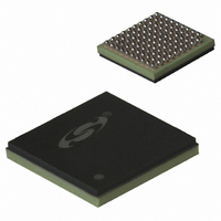
... Si5364 4. Ordering Guide Part Number Si5364-F-BC 36 Package Temperature 99-Ball CBGA – °C Rev. 2.2 ...
Page 37
... Package Outline Figure 16 illustrates the package details for the Si5364. Table 11 lists the values for the dimensions shown in the illustration. Figure 16. 99-Ball Ceramic Ball Grid Array (CBGA) Table 11. Package Diagram Dimensions Symbol Description A Total Package Height A1 A2 Body Thickness b Solder Ball Diameter ...
Page 38
... Si5364 6. 11x11 mm CBGA Card Layout Placement Courtyard Symbol Parameter C Column Width D Row Height E Pad Pitch F Placement Courtyard X Pad Diameter Notes: 1. The Placement Courtyard is the minimum keep-out area required to assure assembly clearances. 2. Pad Diameter is Copper Defined (Non-Solder Mask Defined/NSMD). 3. OSP Surface Finish Recommended. ...
Page 39
... Update Table 3, “AC Characteristics,” on page 8. Updated Figure 10, “Phase Transient Specification,” on page 19. Updated Table 11, “Package Diagram Dimensions,” on page 37. Added Figure 6, “Typical Si5364 Phase Noise (CLKIN = 19.44 MHz, CLKOUT = 622.08 MHz, and Loop BW = 800 Hz),” on page 14. Revision 2.1 to Revision 2.2 Updated "2.7. Reset" on page 21. ...
Page 40
... Si5364 C I ONTACT NFORMATION Silicon Laboratories Inc. 4635 Boston Lane Austin, TX 78735 Tel: 1+(512) 416-8500 Fax: 1+(512) 416-9669 Toll Free: 1+(877) 444-3032 Email: productinfo@silabs.com Internet: www.silabs.com The information in this document is believed to be accurate in all respects at the time of publication but is subject to change without notice. ...