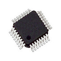
IDT5V9885BPFGI IDT, Integrated Device Technology Inc, IDT5V9885BPFGI Datasheet - Page 22

IDT5V9885BPFGI
Manufacturer Part Number
IDT5V9885BPFGI
Description
IC CLK GEN 3.3V EEPROM 32-TQFP
Manufacturer
IDT, Integrated Device Technology Inc
Type
Clock Generatorr
Datasheet
1.IDT5V9885BNLGI.pdf
(37 pages)
Specifications of IDT5V9885BPFGI
Pll
Yes with Bypass
Input
LVCMOS, LVTTL, Crystal
Output
LVCMOS, LVDS, LVPECL, LVTTL
Number Of Circuits
1
Ratio - Input:output
2:8
Differential - Input:output
No/Yes
Frequency - Max
500MHz
Divider/multiplier
Yes/Yes
Voltage - Supply
3.135 V ~ 3.6 V
Operating Temperature
-40°C ~ 85°C
Mounting Type
Surface Mount
Package / Case
32-TQFP, 32-VQFP
Frequency-max
500MHz
Number Of Elements
3
Supply Current
120mA
Pll Input Freq (min)
1MHz
Pll Input Freq (max)
400MHz
Operating Supply Voltage (typ)
3.3V
Operating Temp Range
-40C to 85C
Package Type
TQFP
Output Frequency Range
0.0049 to 500MHz
Operating Supply Voltage (min)
3V
Operating Supply Voltage (max)
3.6V
Operating Temperature Classification
Industrial
Pin Count
32
Lead Free Status / RoHS Status
Lead free / RoHS Compliant
Other names
5V9885BPFGI
Available stocks
Company
Part Number
Manufacturer
Quantity
Price
Company:
Part Number:
IDT5V9885BPFGI
Manufacturer:
IDT, Integrated Device Technology Inc
Quantity:
10 000
Part Number:
IDT5V9885BPFGI
Manufacturer:
IDT
Quantity:
20 000
Company:
Part Number:
IDT5V9885BPFGI8
Manufacturer:
IDT, Integrated Device Technology Inc
Quantity:
10 000
PROGRAMMING THE DEVICE
to be LOW for I
I
byte of data after a write frame to the correct slave address is interpreted as the register address; this address auto-increments after each byte written or read.
The frame formats are shown below.
2
IDT5V9885B
3.3V EEPROM PROGRAMMABLE CLOCK GENERATOR
C PROGRAMMING
I
Hardwired Parameters for the IDT5V9885B
JTAG identification number = 32'b0000_0000001110101100_00000110011_1
Device (slave) address = 7'b1101010
ID Byte for the 5V9885B = 8'b00010000
The 5V9885B is programmed through an I
Each frame starts with a "Start Condition" and ends with an "End Condition". These are both generated by the Master device.
2
C and JTAG may be used to program the 5V9885B. The I
2
C mode.
SDA
SCL
The first byte transmitted by the Master is the Slave Address followed by the R/W bit.
The Slave acknowledges by sending a "1" bit.
R/W
0 - Slave will be written by master
1 - Slave will be read by master
Condition
Start
S
2
C-Bus serial interface, and is an I
MSB
1
Figure 2: First Byte Transmittetd on I
1
2
C/JTAG pin selects the I
7-bit slave address
Data is stable during
0
Figure 1: Framing
Data Frame
clock HIGH
1
22
2
0
C slave device. The read and write transfer formats are supported. The first
1
2
C when HIGH and JTAG when LOW. Note that the TRST pin needs
0
2
C Bus
LSB
R/W
ACK from Slave
Condition
Stop
P
INDUSTRIAL TEMPERATURE RANGE
SDA
SCL


