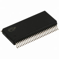
CY28RS400ZXCT Cypress Semiconductor Corp, CY28RS400ZXCT Datasheet - Page 9

CY28RS400ZXCT
Manufacturer Part Number
CY28RS400ZXCT
Description
IC CLOCK GENERATOR 56-TSSOP
Manufacturer
Cypress Semiconductor Corp
Type
Clock Generatorr
Datasheet
1.CY28RS400OXC.pdf
(19 pages)
Specifications of CY28RS400ZXCT
Frequency - Max
100MHz
Voltage - Supply
3.135 V ~ 3.465 V
Operating Temperature
0°C ~ 70°C
Mounting Type
Surface Mount
Package / Case
56-TSSOP II
Frequency-max
100MHz
Lead Free Status / RoHS Status
Lead free / RoHS Compliant
Output
-
Input
-
Document #: 38-07637 Rev. *B
As mentioned previously, the capacitance on each side of the
crystal is in series with the crystal. This mean the total capac-
itance on each side of the crystal must be twice the specified
load capacitance (CL). While the capacitance on each side of
the crystal is in series with the crystal, trim capacitors
(Ce1,Ce2) should be calculated to provide equal capacitance
loading on both sides.
Use the following formulas to calculate the trim capacitor
values for Ce1 and Ce2.
CL ................................................... Crystal load capacitance
CLe .........................................Actual loading seen by crystal
using standard value trim capacitors
Ce .....................................................External trim capacitors
Cs.............................................. Stray capacitance (terraced)
Ci ........................................................... Internal capacitance
(lead frame, bond wires etc.)
CLe
Total Capacitance (as seen by the crystal)
=
(
Load Capacitance (each side)
Ce1 + Cs1 + Ci1
Ce = 2 * CL – (Cs + Ci)
CPUC, 133MHz
CPUT, 133MHz
SRCC 100MHz
SRCT 100MHz
1
PCI, 33 MHz
USB, 48MHz
DOT96C
DOT96T
REF
PD
+
1
Figure 3. Power-down Assertion Timing Waveform
Ce2 + Cs2 + Ci2
1
)
PD (Power-down) Clarification
The VTT_PWRGD# /PD pin is a dual function pin. During initial
power up, the pin functions as VTT_PWRGD#. Once
VTT_PWRGD# has been sampled low by the clock chip, the
pin assumes PD functionality. The PD pin is an asynchronous
active high input used to shut off all clocks cleanly prior to
shutting off power to the device. This signal is synchronized
internal to the device prior to powering down the clock synthe-
sizer. PD is also an asynchronous input for powering up the
system. When PD is asserted high, all clocks need to be driven
to a low value and held prior to turning off the VCOs and the
crystal oscillator.
PD (Power-down) – Assertion
When PD is sampled high by two consecutive rising edges of
CPUC, all single-ended outputs will be held low on their next
high to low transition and differential clocks must held high or
Hi-Zd (depending on the state of the control register drive
mode bit) on the next diff clock# high to low transition within
four clock periods. When the SMBus PD drive mode bit corre-
sponding to the differential (CPU, SRC, and DOT) clock output
of interest is programmed to ‘0’, the clock output are held with
“Diff clock” pin driven high at 2 x Iref, and “Diff clock#” tristate.
If the control register PD drive mode bit corresponding to the
output of interest is programmed to “1”, then both the “Diff
clock” and the “Diff clock#” are three-state. Note the example
below shows CPUT = 133 MHz and PD drive mode = ‘1’ for all
differential outputs. This diagram and description is applicable
to valid CPU frequencies 100,133,200 and 266MHz. In the
event that PD mode is desired as the initial power-on state, PD
must be asserted high in less than 10 uS after asserting
Vtt_PwrGd#.
PD Deassertion
The power-up latency is less than 1.8 ms. This is the time from
the deassertion of the PD pin or the ramping of the power
supply until the time that stable clocks are output from the
clock chip. All differential outputs stopped in a three-state
condition resulting from power down will be driven high in less
than 300 µs of PD deassertion to a voltage greater than 200
mV. After the clock chip’s internal PLL is powered up and
locked, all outputs will be enabled within a few clock cycles of
each other. Below is an example showing the relationship of
clocks coming up.
CY28RS400
Page 9 of 19
[+] Feedback


