CY28RS400ZXCT Cypress Semiconductor Corp, CY28RS400ZXCT Datasheet - Page 3
CY28RS400ZXCT
Manufacturer Part Number
CY28RS400ZXCT
Description
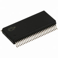
IC CLOCK GENERATOR 56-TSSOP
Manufacturer
Cypress Semiconductor Corp
Type
Clock Generatorr
Datasheet
1.CY28RS400OXC.pdf
(19 pages)
Specifications of CY28RS400ZXCT
Frequency - Max
100MHz
Voltage - Supply
3.135 V ~ 3.465 V
Operating Temperature
0°C ~ 70°C
Mounting Type
Surface Mount
Package / Case
56-TSSOP II
Frequency-max
100MHz
Lead Free Status / RoHS Status
Lead free / RoHS Compliant
Output
-
Input
-


Document #: 38-07637 Rev. *B
Frequency Select Pins (FS_A, FS_B, FS_C and
409_410)
Host clock frequency selection is achieved by applying the
appropriate logic levels to FS_A, FS_B, FS_C and 409_410
inputs prior to VTT_PWRGD# assertion (as seen by the clock
synthesizer). Upon VTT_PWRGD# being sampled low by the
clock chip (indicating processor VTT voltage is stable), the
clock chip samples the FS_A, FS_B, FS_C and 409_410 input
values. For all logic levels of FS_A, FS_B, FS_C and 409_410
VTT_PWRGD# employs a one-shot functionality in that once
Table 1. Frequency Select Table (FS_A FS_B FS_C) 410 mode, 409_410 = 0
Table 2. Frequency Select Table (FS_A FS_B) 410 mode, 409_410 = 1
Serial Data Interface
To enhance the flexibility and function of the clock synthesizer,
a two-signal serial interface is provided. Through the Serial
Data Interface, various device functions, such as individual
clock output buffers, can be individually enabled or disabled.
The registers associated with the Serial Data Interface
initializes to their default setting upon power-up, and therefore
use of this interface is optional. Clock device register changes
are normally made upon system initialization, if any are
required. The interface cannot be used during system
operation for power management functions.
Table 3. Command Code Definition
Table 4. Block Read and Block Write Protocol
FS_C
FS_B
18:11
(6:5)
(4:0)
8:2
Bit
Bit
10
19
1
0
0
0
1
0
0
1
1
9
7
Start
Slave address – 7 bits
Write
Acknowledge from slave
Command Code – 8 bits
Acknowledge from slave
0 = Block read or block write operation, 1 = Byte read or byte write operation
Chip select address, set to ‘00’ to access device
Byte offset for byte read or byte write operation. For block read or block write operations, these bits should be '00000'
FS_B
FS_A
0
0
1
0
1
0
1
0
Block Write Protocol
FS_A
1
1
0
0
1
100 MHz
133 MHz
200 MHz
Description
CPU
Reserved
100 MHz
133 MHz
200 MHz
266 MHz
CPU
100 MHz
100 MHz
100 MHz
SRC
100 MHz
100 MHz
100 MHz
100 MHz
100 MHz
SRC
Description
a valid low on VTT_PWRGD# has been sampled, all further
VTT_PWRGD#, FS_A, FS_B, FS_C and 409-410 transitions
will be ignored. There are 2 CPU frequency select tables. One
based on the CK409 specifications and one based on the
CK410 specifications. The table to be used is determined by
the value latched on the PCI0/409_410 pin by the
VTT_PWRGD/PD# pin. A '0' on this pin selects the 410
frequency table and a '1' on this pin selects the 409 frequency
table. In the 409 table, only the FS_A and FS_B pins influence
the frequency selection.
Data Protocol
The clock driver serial protocol accepts byte write, byte read,
block write, and block read operations from the controller. For
block write/read operation, the bytes must be accessed in
sequential order from lowest to highest byte (most significant
bit first) with the ability to stop after any complete byte has
been transferred. For byte write and byte read operations, the
system controller can access individually indexed bytes. The
offset of the indexed byte is encoded in the command code,
as described in Table 3.
The block write and block read protocol is outlined in Table 4
while Table 5 outlines the corresponding byte write and byte
read protocol. The slave receiver address is 11010010 (D2h).
18:11
Bit
8:2
10
19
1
9
PCIF/PCI
33 MHz
33 MHz
33 MHz
PCIF/PCI
33 MHz
33 MHz
33 MHz
33 MHz
33 MHz
Start
Slave address – 7 bits
Write
Acknowledge from slave
Command Code – 8 bits
Acknowledge from slave
Block Read Protocol
14.318 MHz
14.318 MHz
14.318 MHz
14.318 MHz
14.318 MHz
14.318 MHz
14.318 MHz
14.318 MHz
REF0
Description
REF0
CY28RS400
48 MHz
48 MHz
48 MHz
Page 3 of 19
48 MHz
48 MHz
48 MHz
48 MHz
48 MHz
USB
USB
[+] Feedback
Related parts for CY28RS400ZXCT
Image
Part Number
Description
Manufacturer
Datasheet
Request
R

Part Number:
Description:
Manufacturer:
Cypress Semiconductor Corp
Datasheet:
Part Number:
Description:
Manufacturer:
Cypress Semiconductor Corp
Datasheet:
Part Number:
Description:
Manufacturer:
Cypress Semiconductor Corp
Datasheet:
Part Number:
Description:
Manufacturer:
Cypress Semiconductor Corp
Datasheet:
Part Number:
Description:
Manufacturer:
Cypress Semiconductor Corp
Datasheet: