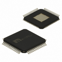
SY89538LHG TR Micrel Inc, SY89538LHG TR Datasheet - Page 10

SY89538LHG TR
Manufacturer Part Number
SY89538LHG TR
Description
IC SYNTHESIZR LVPECL/LVDS 64TQFP
Manufacturer
Micrel Inc
Series
Precision Edge®r
Type
Clock Synthesizer/Fanout Bufferr
Datasheet
1.SY89538LHH.pdf
(23 pages)
Specifications of SY89538LHG TR
Pll
Yes
Input
CMOS, HSTL, LVDS, LVPECL, LVTTL, SSTL, Crystal
Output
LVDS, LVPECL
Number Of Circuits
1
Ratio - Input:output
2:7
Differential - Input:output
Yes/Yes
Frequency - Max
756MHz
Divider/multiplier
Yes/No
Voltage - Supply
2.375 V ~ 3.6 V
Operating Temperature
-40°C ~ 85°C
Mounting Type
Surface Mount
Package / Case
64-TQFP Exposed Pad, 64-eTQFP, 64-HTQFP, 64-VQFP
Frequency-max
756MHz
Lead Free Status / RoHS Status
Lead free / RoHS Compliant
Other names
SY89538LHGTR
SY89538LHGTR
SY89538LHGTR
AC Electrical Characteristics
V
(LVPECL) = 50Ω into V
Notes:
7.
8.
9.
10. Total jitter definition: with an ideal clock input of frequency <f
11. Crosstalk is measured at the output while applying two similar differential clock frequencies that are asynchronous with respect to each
June 2006
Symbol
f
f
f
f
t
t
t
BW
t
t
t
t
CCA
IN
REF
OUT
VCO
SKEW
LOCK
JITTER
DC
r,
PW_SYNC_MIN
PD_SYNC
t
f
Fundamental mode, series resonant crystal.
The output-to-output skew is defined as the worst-case difference between any outputs within a single device operating at the same voltage
and temperature.
Cycle-to-cycle jitter definition: the variation of periods between adjacent cycles, T
output signal.
than the specified peak-to-peak jitter value.
other at the inputs.
= V
CCD
= +3.3V ±10%; V
Parameter
XTAL Input Frequency Range
Reference Input Frequency Range
Zero Delay Input Frequency Range
Phase Detector Operating
Frequency Range
Output Frequency Range
Internal VCO Frequency Range
Output-to-Output
Minimum PLL Lock Time
Loop Filter Optimized for Cycle-to-Cycle Jitter
• R = 50Ω
• C1 = 0.47µF
• C2 = 1000pF
1-Sigma Cycle-to-Cycle Jitter (XTAL Input)
1-Sigma Cycle-to-Cycle Jitter (RFCK Reference)
Total Jitter
Spur
XTAL/RFCK Crosstalk-Induced Jitter
PLL Bandwidth
F
Output Rise/Fall Time (20% to 80%)
Output Rise/Fall Time (20% to 80%)
Minimum SYNC Pulse Width
Synchronization Delay
OUT
Duty Cycle
CCO
–2V; T
CCO
A
= +2.5V ±5% or +3.3V ±10%, R
= –40°C to +85°C, unless otherwise stated.
MAX
, no more than one output edge in 10
10
Condition
Note 7
See Table 8
See Table 9
INSEL = LOW
INSEL = HIGH
Note 8
Note 9
Note 9
Note 10
Note 11
See Table 10
14 ≤ f
LVPECL
LVDS
See “Synchronization”
section
See “Synchronization”
section
REF
L
(LVDS) = 100Ω across the output pairs, R
≤ 18
n
– T
n-1
where T is the time between rising edges of the
hbwhelp@micrel.com
29.375
29.375
9.325
9.325
12
2352
11.1
Min
100
14
14
43
80
output edges will deviate by more
8
Typ
250
150
-35
15
80
50
4
5
8
or (408) 955-1690
M9999-062706-D
3024
Max
94.5
38.4
756
756
756
150
400
300
0.7
18
18
75
10
14
57
6
L
Internal
Internal
ps
ps
ps
Units
fphase
clock
cycle
clock
cycle
dBc@
MHz
MHz
MHz
MHz
MHz
MHz
MHz
ps
kHz
ms
ps
ps
ps
%
RMS
RMS
RMS
PP


