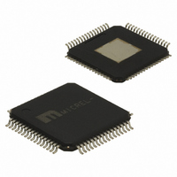
SY89538LHG TR Micrel Inc, SY89538LHG TR Datasheet

SY89538LHG TR
Specifications of SY89538LHG TR
SY89538LHGTR
Related parts for SY89538LHG TR
SY89538LHG TR Summary of contents
Page 1
... Precision Edge is a registered trademark of Micrel, Inc. MLF and MicroLeadFrame are registered trademarks of Amkor Technology. Micrel Inc. • 2180 Fortune Drive • San Jose, CA 95131 • USA • tel +1 (408) 944-0800 • fax + 1 (408) 474-1000 • http://www.micrel.com June 2006 Programmable Multiple Output Bank Clock ...
Page 2
Typical Application Functional Block Diagram June 2006 2 hbwhelp@micrel.com M9999-062706-D or (408) 955-1690 ...
Page 3
Ordering Information Part Number Package Type SY89538LHG H64-1 (2) SY89538LHGTR H64-1 Notes: 1. Contact factory for die availability. Dice are guaranteed Tape and Reel. Pin Configuration June 2006 Operating Package Marking Range Industrial SY89538LHG with Pb-Free ...
Page 4
Pin Description Power Pin Number Pin Name 1 VCCA VCCD 6, 56 19, 40, 43, 51 VCCO 15 GNDA 16, 30, 31, GND, 47, 55 Exposed Pad Control and Configuration Pin Number Pin Name ...
Page 5
Pin Description Control and Configuration (continued) Pin Number Pin Name 24 PEN0 26 PEN1 58 PEN2 60 PEN3 46 SYNC 5 FBSEL 28 PD_4 33 PD_2 35 PD_0 27 PD_5 29 PD_3 34 PD_1 13, 14 PDSEL1, PDSEL0 22 DSEL ...
Page 6
Pin Description Input/Output Pin Number Pin Name 3, 4 FBIN, /FBIN 8, 9 RFCK, /RFCK XTAL2, XTAL1 11, 12 17, 18 POUT0, /POUT0 20, 21 POUT1, /POUT1 49, 50 POUT2, /POUT2 52, 53 POUT3, /POUT3 38, 39 LOUT0, /LOUT0 LOUT1, ...
Page 7
Output and Frequency Select Tables PSELx Table 3. LVPECL Output Post-Divider and Frequency Select Table LSEL Table 4. LVDS Output Post-Divider and Frequency Select ...
Page 8
Absolute Maximum Ratings Supply Voltage ( CCD CCA CCO Input Voltage (RFCK, FBIN)................... –0. XTAL Input Voltage (V ) ......... V XTAL1, 2 Output Current (I ) OUT LVPECL Outputs (Surge) .........................100mA LVPECL Outputs ...
Page 9
Reference Clock Inputs/External Feedback Inputs +3.3V ±10%, V CCA CCD CCO Symbol Parameter V Input HIGH Voltage IH V Input LOW Voltage IL V Input Voltage Swing IN V Differential Input Voltage Swing DIFF_IN 100K LVPECL ...
Page 10
AC Electrical Characteristics +3.3V ±10%; V CCA CCD CCO (LVPECL) = 50Ω into V –2V; T CCO Symbol Parameter XTAL Input Frequency Range f Reference Input Frequency Range IN Zero Delay Input Frequency Range Phase Detector ...
Page 11
Single-Ended and Differential Swings Figure 1a. Single-Ended Voltage Swing June 2006 Figure 1b. Differential Voltage Swing 11 hbwhelp@micrel.com M9999-062706-D or (408) 955-1690 ...
Page 12
Functional Description Overall Function The SY89538L integrated synthesizer and fanout buffer with zero delay is part of a precision PLL-based clock generation family optimized for internal system clock generation (FPGAs, ASICs, NPU). Inputs XTAL The SY89538L features a fully integrated ...
Page 13
Table 8 summarizes the input reference frequency and associated divider values: f (MHz) RFCK Ref-Div = 1 Ref-Div = 8 73.5 756 65.3 672 58.8 605 53.5 550 49.0 504 … … 14.7 151 14.3 148 14.0 144 13.7 141 ...
Page 14
Zero Delay FBIN Input The SY89538L features a zero delay MUX that forces the output the same phase relationship as the reference. This effectively configures the SY89538L as a zero delay buffer when FBSEL is logic HIGH ...
Page 15
Post- Pre- VCO Divider Divider Min. Max. 2.35 3. 2.35 3. 2.35 3. 2.35 3. 2.35 3. 2.35 3. 2.35 3. 2.35 3.02 2 ...
Page 16
External Loop Filter Considerations The SY89538L features an external PLL loop filter that allows the users to tailor the PLL’s behavior recommended that ceramic capacitors with NPO or X7R dielectric be used, since they have very low effective ...
Page 17
Synchronization Output Synchronization Controlled by SYNC Timing Diagram The SYNC control input is used to synchronize all divider outputs of the post divider. When a HIGH-LOW transition is applied to the SYNC control input the outputs are disabled when all ...
Page 18
PLL Loop Stability For the loop filter configurations shown in Figure 4, Table 10 below summarizes the PLL’s loop stability in terms of damping factor, natural frequency, and bandwidth, and illustrates the pole and zero cutoff Parameter Vcc 3 3 ...
Page 19
Figure 6 shows the open and closed loop gain of the SY89538L. The closed loop-gain plot shows that the SY89538L when configured with the recommended loop filter values has essentially no jitter peaking near the -3dB point. In addition, the ...
Page 20
Input Termination (RFCK and FBIN) Figure 11a. LVPECL Interface (DC-Coupled) Figure 11d. CML Interface (AC-Coupled) Figure 11g. 2.5V CML (DC-Coupled) June 2006 Figure 11b. LVPECL Interface (AC-Coupled) Figure 11e. LVDS (DC-Coupled) Figure 11h. Single-Ended Input Interface 20 Figure 11c. CML ...
Page 21
Output Bank and Frequency Control There are five independently programmable output frequency banks, four differential LVPECL output banks and one differential LVDS output bank with three output pairs. Each bank has frequency control DSEL, SELx and Enx to generate different ...
Page 22
LVDS LVDS specifies a small swing of 325mV typical nominal 1.2V common mode above ground. The common mode voltage has tight limits to permit large variations in ground between an LVDS driver and receiver. Also, change in common ...
Page 23
Package Information MICREL, INC. 2180 FORTUNE DRIVE SAN JOSE, CA 95131 USA TEL +1 (408) 944-0800 FAX +1 (408) 474-1000 WEB http:/www.micrel.com The information furnished by Micrel in this data sheet is believed to be accurate and reliable. However, no ...


