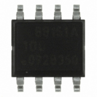
MB88151APNF-G-100-JNE1 Fujitsu Semiconductor America Inc, MB88151APNF-G-100-JNE1 Datasheet

MB88151APNF-G-100-JNE1
Specifications of MB88151APNF-G-100-JNE1
Related parts for MB88151APNF-G-100-JNE1
MB88151APNF-G-100-JNE1 Summary of contents
Page 1
FUJITSU MICROELECTRONICS DATA SHEET ASSP Spread Spectrum Clock Generator MB88151A ■ DESCRIPTION MB88151A is a clock generator for EMI (Electro Magnetic Interference) reduction. The peak of unnecessary radiation noise (EMI) can be attenuated by making the oscillation frequency slightly modulate ...
Page 2
MB88151A ■ PRODUCT LINEUP MB88151A has five kinds of multiplication type. Product Input frequency range MB88151A-100/101 MB88151A-200/201 16.6 MHz to 33.4 MHz MB88151A-400/401 MB88151A-500/501 MB88151A-800/801 8.3 MHz to 16.7 MHz ■ PIN ASSIGNMENT ■ PIN DESCRIPTION Pin name I/O Pin ...
Page 3
I/O CIRCUIT TYPE Pin SEL0, SEL1 ENS CKOUT Note : For XIN and XOUT pins, refer to “■OSCILLATION CIRCUIT”. DS04-29127-2E Circuit type CMOS hysteresis input CMOS hysteresis input with 50 kΩ + 800 kΩ (Typ) pull-up resistors 50 kΩ ...
Page 4
MB88151A ■ HANDLING DEVICES Preventing Latch-up A latch-up can occur if, on this device, (a) a voltage higher than V input or output pin or (b) a voltage higher than the rating is applied between occurs, significantly ...
Page 5
BLOCK DIAGRAM Modulation rate setting SEL1 Modulation rate setting SEL0 Modulation enable setting/ Power down setting ENS/XPD Reference clock XOUT = 1 MΩ XIN − Reference clock − − glitchless ...
Page 6
MB88151A ■ PIN SETTING When changing the pin setting, the stabilization wait time for the modulation clock is required. The stabilization wait time for the modulation clock take the maximum value of “■ ELECTRICAL CHARACTERISTICS • AC Characteristics Lock-up time”. ...
Page 7
Center spread Spectrum is spread (modulated) by centering on the frequency in modulation off. Radiation level Center spread example of ± 1.5% modulation rate • Down spread Spectrum is spread (modulated) below the frequency in modulation off. Modulation width ...
Page 8
MB88151A ■ ABSOLUTE MAXIMUM RATINGS Parameter Power supply voltage* Input voltage* Output voltage* Storage temperature Operation junction temperature Output current Overshoot Undershoot = 0 The parameter is based WARNING: Semiconductor devices can be permanently ...
Page 9
RECOMMENDED OPERATING CONDITIONS Parameter Symbol Power supply voltage V DD “H” level input voltage V IH “L” level input voltage V IL Input clock t DCI duty cycle Operating temperature Ta WARNING: The recommended operating conditions are required in ...
Page 10
MB88151A ■ ELECTRICAL CHARACTERISTICS • DC Characteristics Parameter Symbol Power supply current Output voltage V OL Output impedance Z O Input capacitance C IN Load capacitance PUE Input pull-up resistance R PUP 10 ...
Page 11
AC Characteristics Parameter Symbol Oscillation frequency f x Input frequency f in Output frequency f OUT Output slew rate SR Output clock duty cycle t DCC Modulation period f MOD (Number of input clocks (n ) MOD per modulation) ...
Page 12
MB88151A < Definition of modulation frequency and number of input clocks per modulation f (Output frequency) MB88151A contains the modulation period to realize the efficient EMI reduction. The modulation period f depends on the input frequency and changes between f ...
Page 13
OUTPUT CLOCK DUTY CYCLE (t CKOUT ■ INPUT FREQUENCY (f = 1/t in XIN ■ OUTPUT SLEW RATE (SR) CKOUT t r Note : SR = (2.4 − 0. (2.4 − 0. ■ ...
Page 14
MB88151A ■ MODULATION WAVEFORM • ±1.5% modulation rate, Example of center spread CKOUT Output frequency + 1.5 % Frequency at modulation OFF − 1.5 % • −1.0% modulation rate, Example of down spread CKOUT Output frequency Frequency at modulation OFF ...
Page 15
LOCK-UP TIME 3 XIN Setting pin V SEL0, SEL1, ENS CKOUT If the setting pin is fixed at the “H” or “L” level, the maximum time after the power is turned on until the set clock ...
Page 16
MB88151A XIN XPD CKOUT When the power down is controlled by XPD pin, the desired clock is obtained after the pin is set to H level until the maximum lock-up time t is elapsed Internal clock stabilization wait ...
Page 17
OSCILLATION CIRCUIT The figure below shows the connection example about general resonator. The oscillation circuit has the built-in resistance (1 MΩ) . The value of capacity (C resonator. The most suitable value is different by individual resonator. Please refer ...
Page 18
MB88151A ■ INTERCONNECTION CIRCUIT EXAMPLE C 1 SEL0 SEL1 Oscillation stabilization capacitance (refer to “■OSCILLATION CIRCUIT”.) Capacitor of 10 µF or higher Capacitor about 0.01 µF (connect a capacitor of ...
Page 19
SPECTRUM EXAMPLE CHARACTERISTICS The condition of the examples of the characteristic is shown as follows : Input frequency = 20 MHz (Output frequency = 20 MHz : Using MB88151A-100 (Multiply-by-1)), Power - supply voltage = 3.3 V, None load ...
Page 20
... MB88151A ■ ORDERING INFORMATION Input frequency Part number MB88151APNF-G-100-JNE1 MB88151APNF-G-101-JNE1 MB88151APNF-G-200-JNE1 MB88151APNF-G-201-JNE1 16.6 MHz to MB88151APNF-G-400-JNE1 MB88151APNF-G-401-JNE1 MB88151APNF-G-500-JNE1 MB88151APNF-G-501-JNE1 MB88151APNF-G-800-JNE1 8.3 MHz to MB88151APNF-G-801-JNE1 MB88151APNF-G-100-JNEFE1 MB88151APNF-G-101-JNEFE1 MB88151APNF-G-200-JNEFE1 MB88151APNF-G-201-JNEFE1 16.6 MHz to MB88151APNF-G-400-JNEFE1 MB88151APNF-G-401-JNEFE1 MB88151APNF-G-500-JNEFE1 MB88151APNF-G-501-JNEFE1 MB88151APNF-G-800-JNEFE1 8.3 MHz to MB88151APNF-G-801-JNEFE1 MB88151APNF-G-100-JNERE1 MB88151APNF-G-101-JNERE1 MB88151APNF-G-200-JNERE1 MB88151APNF-G-201-JNERE1 16.6 MHz to ...
Page 21
PACKAGE DIMENSION 8-pin plastic SOP (FPT-8P-M02) 8-pin plastic SOP (FPT-8P-M02) +0.25 +.010 1 * 5.05 .199 –0.20 –.008 1.27(.050) 0.44±0.08 (.017±.003) 0.10(.004) 0.10(.004) ©2002-2008 FUJITSU MICROELECTRONICS LIMITED F08004S-c-4-8 2002 FUJITSU LIMITED F08004S-c-4-7 C Please confirm ...
Page 22
MB88151A ■ MAIN CHANGES IN THIS EDITION Page Section ⎯ ⎯ 22 Change Results Preliminary Data Sheet → Data Sheet DS04-29127-2E ...
Page 23
MEMO DS04-29127-2E MB88151A 23 ...
Page 24
MB88151A FUJITSU MICROELECTRONICS LIMITED Shinjuku Dai-Ichi Seimei Bldg., 7-1, Nishishinjuku 2-chome, Shinjuku-ku, Tokyo 163-0722, Japan Tel: +81-3-5322-3347 Fax: +81-3-5322-3387 http://jp.fujitsu.com/fml/en/ For further information please contact: North and South America FUJITSU MICROELECTRONICS AMERICA, INC. 1250 E. Arques Avenue, M/S 333 Sunnyvale, ...


