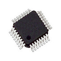
MC100ES6226AC IDT, Integrated Device Technology Inc, MC100ES6226AC Datasheet - Page 7

MC100ES6226AC
Manufacturer Part Number
MC100ES6226AC
Description
IC CLK DIVIDER FAN BUFF 32LQFP
Manufacturer
IDT, Integrated Device Technology Inc
Type
Fanout Buffer (Distribution), Dividerr
Series
100ESr
Datasheet
1.MC100ES6226AC.pdf
(9 pages)
Specifications of MC100ES6226AC
Number Of Circuits
1
Ratio - Input:output
1:9
Differential - Input:output
Yes/Yes
Input
LVCMOS, LVPECL
Output
LVPECL
Frequency - Max
3GHz
Voltage - Supply
2.375 V ~ 3.465 V
Operating Temperature
0°C ~ 110°C
Mounting Type
Surface Mount
Package / Case
32-LQFP
Frequency-max
3GHz
Number Of Clock Inputs
1
Mode Of Operation
Differential
Output Frequency
3000MHz
Output Logic Level
LVPECL
Operating Supply Voltage (min)
2.375V
Operating Supply Voltage (typ)
2.5/3.3V
Operating Supply Voltage (max)
3.465V
Package Type
TQFP
Operating Temp Range
0C to 110C
Operating Temperature Classification
Commercial
Signal Type
LVPECL
Mounting
Surface Mount
Pin Count
32
Lead Free Status / RoHS Status
Lead free / RoHS Compliant
Other names
800-2002
MC100ES6226ACIDT
MC100ES6226ACIDT
Available stocks
Company
Part Number
Manufacturer
Quantity
Price
Company:
Part Number:
MC100ES6226AC
Manufacturer:
ON
Quantity:
184
Company:
Part Number:
MC100ES6226AC
Manufacturer:
IDT, Integrated Device Technology Inc
Quantity:
10 000
Company:
Part Number:
MC100ES6226ACR2
Manufacturer:
IDT, Integrated Device Technology Inc
Quantity:
10 000
Maintaining Lowest Device Skew
skew of 35 ps and a part-to-part skew of max. TBD ps. To ensure
low skew clock signals in the application, both outputs of any
differential output pair need to be terminated identically, even if
only one output is used. When fewer than all nine output pairs are
used, identical termination of all output pairs within the output
bank is recommended. If an entire output bank is not used, it is
recommended to leave all of these outputs open and
unterminated. This will reduce the device power consumption
while maintaining minimum output skew.
Power Supply Bypassing
differential architecture of the MC100ES6226 supports low noise
signal operation at high frequencies. In order to maintain its
superior signal quality, all V
IDT™ / ICS™ CLOCK DISTRIBUTION BUFFER/CLOCK DRIVER
MC100ES6226
2.5V/3.3V DIFFERENTIAL LVPECL 1:9 CLOCK DISTRIBUTION BUFFER AND CLOCK DRIVER
The MC100ES6226 guarantees low output-to-output bank
The MC100ES6226 is a mixed analog/digital product. The
Differential Pulse
Generator
Z = 50 Ω
CC
pins should be bypassed by
Z
O
= 50 Ω
R
V
T
TT
= 50 Ω
Figure 4. MC100ES6226 AC Test Reference
APPLICATIONS INFORMATION
MC100ES6226
DUT
7
high-frequency ceramic capacitors connected to GND. If the
spectral frequencies of the internally generated switching noise on
the supply pins cross the series resonant point of an individual
bypass capacitor, its overall impedance begins to look inductive
and thus increases with increasing frequency. The parallel
capacitor combination shown ensures that a low impedance path
to ground exists for frequencies well above the noise bandwidth.
Z
O
V
= 50 Ω
CC
R
T
= 50 Ω
Figure 5. V
33...100 nF
MC100ES6226 REV. 5 NOVEMBER 10, 2008
CC
Power Supply Bypass
V
TT
0.1 nF
V
CC
MC100ES6226


