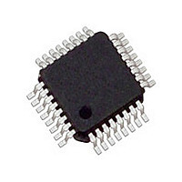
MC100ES6226AC IDT, Integrated Device Technology Inc, MC100ES6226AC Datasheet - Page 6

MC100ES6226AC
Manufacturer Part Number
MC100ES6226AC
Description
IC CLK DIVIDER FAN BUFF 32LQFP
Manufacturer
IDT, Integrated Device Technology Inc
Type
Fanout Buffer (Distribution), Dividerr
Series
100ESr
Datasheet
1.MC100ES6226AC.pdf
(9 pages)
Specifications of MC100ES6226AC
Number Of Circuits
1
Ratio - Input:output
1:9
Differential - Input:output
Yes/Yes
Input
LVCMOS, LVPECL
Output
LVPECL
Frequency - Max
3GHz
Voltage - Supply
2.375 V ~ 3.465 V
Operating Temperature
0°C ~ 110°C
Mounting Type
Surface Mount
Package / Case
32-LQFP
Frequency-max
3GHz
Number Of Clock Inputs
1
Mode Of Operation
Differential
Output Frequency
3000MHz
Output Logic Level
LVPECL
Operating Supply Voltage (min)
2.375V
Operating Supply Voltage (typ)
2.5/3.3V
Operating Supply Voltage (max)
3.465V
Package Type
TQFP
Operating Temp Range
0C to 110C
Operating Temperature Classification
Commercial
Signal Type
LVPECL
Mounting
Surface Mount
Pin Count
32
Lead Free Status / RoHS Status
Lead free / RoHS Compliant
Other names
800-2002
MC100ES6226ACIDT
MC100ES6226ACIDT
Available stocks
Company
Part Number
Manufacturer
Quantity
Price
Company:
Part Number:
MC100ES6226AC
Manufacturer:
ON
Quantity:
184
Company:
Part Number:
MC100ES6226AC
Manufacturer:
IDT, Integrated Device Technology Inc
Quantity:
10 000
Company:
Part Number:
MC100ES6226ACR2
Manufacturer:
IDT, Integrated Device Technology Inc
Quantity:
10 000
Table 7. AC Characteristics (V
IDT™ / ICS™ CLOCK DISTRIBUTION BUFFER/CLOCK DRIVER
1. AC characteristics are design targets and pending characterization.
2. AC characteristics apply for parallel output termination of 50 Ω to V
3. V
4. V
5. The MC100ES6226 is fully operational up to 3.0 GHz and is characterized up to 2.7 GHz.
6. Propagation delay OE deassertion to differential output disabled (differential low: true output low, complementary output high).
7. Propagation delay OE assertion to output enabled (active).
Symbol
V
MC100ES6226
2.5V/3.3V DIFFERENTIAL LVPECL 1:9 CLOCK DISTRIBUTION BUFFER AND CLOCK DRIVER
V
t
t
t
t
V
JIT(CC)
PDL
PLD
t
sk(PP)
DC
O(P-P)
f
V
X,OUT
sk(O)
t
t
CLK
range and the input swing lies within the V
device and part-to-part skew.
CMR
r
PD
, t
PP
PP
CMR
O
(6)
(7)
f
is the minimum differential input voltage swing required to maintain AC characteristics including tpd and device-to-device skew.
CLK
CLK
OE
Qx
Qx
(AC) is the crosspoint of the differential input signal. Normal AC operation is obtained when the crosspoint is within the V
Differential Input Voltage
Differential Input Crosspoint Voltage
Differential Output Crosspoint Voltage
Differential Output Voltage (peak-to-peak)
Input Frequency
Propagation Delay CLK to Qx[]
Output-to-Output Skew
Output-to-Output Skew
Output Cycle-to-Cycle Jitter
Output Duty Cycle
Output Rise/Fall Time
Output Disable Time
Output Enable Time
50%
Characteristics
single frequency configuration
÷1/÷2 frequency configuration
t
PDL
CC
(OE to Qx)
(3)
Qx = ÷1, f
Qx = ÷1, f
Qx = ÷2, f
Qx = ÷2, f
= 3.3 V ± 5% and 2.5 V ± 5%, T
(peak-to-peak)
Figure 3. MC100ES6226 Output Disable/Enable Timing
(within QC[2:0])
(within QA[2:0])
(within QB[2:0])
PP
(within device)
f
O
O
O
O
O
f
f
(part-to-part)
(4)
O
O
(AC) specification. Violation of V
< 300 MHz
< 300 MHz
> 300 MHz
< 300 MHz
> 300 MHz
< 1.5 GHz
< 2.7 GHz
RMS (1σ)
V
2.5⋅T + t
3⋅T + t
CC
0.45
TBD
47.5
0.05
Min
475
0.2
1.0
0.3
48
45
49
– 1.45
0
TT
PD
PD
.
J
6
Outputs Disabled
= 0°C to +110°C)
CMR
0.72
0.55
0.37
Typ
500
0.3
11
12
50
50
50
50
(AC) or V
4
t
PLD
PP
(OE to Qx)
(1), (2)
4.5⋅T + t
(AC) impacts the device propagation delay,
V
V
5⋅T + t
3000
CC
CC
Max
0.95
0.95
0.95
52.5
800
325
200
1.3
25
25
20
60
52
55
51
1
1
– 0.3
– 1.1
(5)
PD
PD
MC100ES6226 REV. 5 NOVEMBER 10, 2008
MHz
Unit
ps
ps
ps
ps
ps
ps
ps
ps
ns
ns
ns
%
%
%
%
V
V
V
V
V
V
Differential
Differential
Differential
FSEL0 = FSEL1
FSEL0 ≠ FSEL1
DC
20% to 80%
T = CLK period
T = CLK period
fref
Condition
= 50%
CMR
(AC)


