MC100ES6226AC IDT, Integrated Device Technology Inc, MC100ES6226AC Datasheet - Page 3
MC100ES6226AC
Manufacturer Part Number
MC100ES6226AC
Description
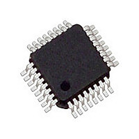
IC CLK DIVIDER FAN BUFF 32LQFP
Manufacturer
IDT, Integrated Device Technology Inc
Type
Fanout Buffer (Distribution), Dividerr
Series
100ESr
Datasheet
1.MC100ES6226AC.pdf
(9 pages)
Specifications of MC100ES6226AC
Number Of Circuits
1
Ratio - Input:output
1:9
Differential - Input:output
Yes/Yes
Input
LVCMOS, LVPECL
Output
LVPECL
Frequency - Max
3GHz
Voltage - Supply
2.375 V ~ 3.465 V
Operating Temperature
0°C ~ 110°C
Mounting Type
Surface Mount
Package / Case
32-LQFP
Frequency-max
3GHz
Number Of Clock Inputs
1
Mode Of Operation
Differential
Output Frequency
3000MHz
Output Logic Level
LVPECL
Operating Supply Voltage (min)
2.375V
Operating Supply Voltage (typ)
2.5/3.3V
Operating Supply Voltage (max)
3.465V
Package Type
TQFP
Operating Temp Range
0C to 110C
Operating Temperature Classification
Commercial
Signal Type
LVPECL
Mounting
Surface Mount
Pin Count
32
Lead Free Status / RoHS Status
Lead free / RoHS Compliant
Other names
800-2002
MC100ES6226ACIDT
MC100ES6226ACIDT
Available stocks
Company
Part Number
Manufacturer
Quantity
Price
Company:

Part Number:
MC100ES6226AC
Manufacturer:
ON
Quantity:
184
Company:
Part Number:
MC100ES6226AC
Manufacturer:
IDT, Integrated Device Technology Inc
Quantity:
10 000
Company:
Part Number:
MC100ES6226ACR2
Manufacturer:
IDT, Integrated Device Technology Inc
Quantity:
10 000


Table 2. Function Table
Table 3. Output Frequency Select Control
IDT™ / ICS™ CLOCK DISTRIBUTION BUFFER/CLOCK DRIVER
OE
MR
FSEL0, FSEL1
MC100ES6226
2.5V/3.3V DIFFERENTIAL LVPECL 1:9 CLOCK DISTRIBUTION BUFFER AND CLOCK DRIVER
Table 1. Pin Configuration
Table 4. Absolute Maximum Ratings
CLK, CLK
OE
MR
FSEL0, FSEL1
QA[0-2], QA[0–2]
QB[0-2], QB[0–2]
QC[0-2], QC[0–2]
GND
V
Control
Symbol
1. Absolute maximum continuous ratings are those maximum values beyond which damage to the device may occur. Exposure to these
FSEL0
CC
V
I
V
V
OUT
I
T
OUT
conditions or conditions beyond those indicated may adversely affect device reliability. Functional operation at absolute-maximum-rated
conditions is not implied.
0
0
1
1
CC
IN
IN
S
Pin
Supply Voltage
DC Input Voltage
DC Output Voltage
DC Input Current
DC Output Current
Storage Temperature
Default
00
0
0
Input
Input
Input
Input
Output
Supply
Supply
FSEL1
I/O
0
1
0
1
Qx[0–2], Qx[0–2] are active. Deassertion of OE can
be asynchronous to the reference clock without
generation of output runt pulses
Normal operation
See
Characteristics
LVPECL
LVCMOS
LVCMOS
LVCMOS
LVPECL
GND
V
CC
Table 3
Type
(1)
Differential reference clock signal input
Output enable
Device reset
Output frequency divider select
Differential clock outputs (banks A, B and C)
Negative power supply
Positive power supply. All V
correct DC and AC operation
f
QA0:2
QA0 to QA2
f
f
f
QA0:2
QA0:2
QA0:2
= f
= f
= f
= f
CLK
CLK
CLK
CLK
0
÷ 2
3
CC
pins must be connected to the positive power supply for
–0.3
–0.3
–0.3
Min
–65
f
f
QB0:2
QB0:2
QB0 to QB2
f
f
QB0:2
QB0:2
Qx[0–2] = L, Qx[0–2] =H (outputs disabled).
Assertion of OE can be asynchronous to the
reference clock without generation of output runt
pulses
Device reset (asynchronous)
= f
= f
= f
= f
CLK
CLK
Function
CLK
CLK
÷ 2
÷ 2
V
V
CC
CC
Max
±20
±50
125
3.6
MC100ES6226 REV. 5 NOVEMBER 10, 2008
+0.3
+0.3
1
f
f
f
QC0:2
QC0:2
QC0:2
QC0 to QC2
f
QC0:2
Unit
mA
mA
= f
= f
= f
°C
V
V
V
= f
CLK
CLK
CLK
CLK
÷ 2
÷ 2
÷ 2
Condition
Related parts for MC100ES6226AC
Image
Part Number
Description
Manufacturer
Datasheet
Request
R

Part Number:
Description:
MICROCOUPLER, SMALL TRANSISTOR OUTPUT
Manufacturer:
Micropac Industries, Inc.
Part Number:
Description:
Steckbare Anschlussklemmen, Raster 5,08 mm
Manufacturer:
LUMBERG [Lumberg]
Datasheet:

Part Number:
Description:
MC100-50805K
Manufacturer:
Cooper/Bussmann
Datasheet:

Part Number:
Description:
TRANSLATION DEVICE DPI 80-PQFP
Manufacturer:
IDT, Integrated Device Technology Inc
Datasheet:
Part Number:
Description:
IDT PART
Manufacturer:
IDT, Integrated Device Technology Inc
Datasheet:
Part Number:
Description:
IC LIU T1/E1/J1 OCTAL 256PBGA
Manufacturer:
IDT, Integrated Device Technology Inc
Datasheet:

Part Number:
Description:
IC FREQ TIMING GENERATOR 28TSSOP
Manufacturer:
IDT, Integrated Device Technology Inc
Datasheet:
Part Number:
Description:
IC CLK DVR PLL 1:10 40VFQFPN
Manufacturer:
IDT, Integrated Device Technology Inc
Datasheet:
Part Number:
Description:
IC CLK FANOUT BUFFER 1:18 32LQFP
Manufacturer:
IDT, Integrated Device Technology Inc
Datasheet:
Part Number:
Description:
IC CLK FANOUT BUFFER 1:18 32LQFP
Manufacturer:
IDT, Integrated Device Technology Inc
Datasheet: