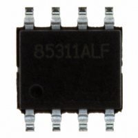
ICS85311AMLF IDT, Integrated Device Technology Inc, ICS85311AMLF Datasheet - Page 7

ICS85311AMLF
Manufacturer Part Number
ICS85311AMLF
Description
IC FANOUT BUFF LVPECL/ECL 8-SOIC
Manufacturer
IDT, Integrated Device Technology Inc
Series
HiPerClockS™r
Type
Fanout Buffer (Distribution)r
Datasheet
1.ICS85311AMLF.pdf
(16 pages)
Specifications of ICS85311AMLF
Number Of Circuits
1
Ratio - Input:output
1:2
Differential - Input:output
Yes/Yes
Input
HCSL, LVDS, LVHSTL, LVPECL, SSTL
Output
ECL, LVPECL
Frequency - Max
1GHz
Voltage - Supply
2.375 V ~ 3.465 V
Operating Temperature
0°C ~ 70°C
Mounting Type
Surface Mount
Package / Case
8-SOIC
Frequency-max
1GHz
Number Of Outputs
4
Operating Supply Voltage (max)
-3.465/3.465V
Operating Temp Range
0C to 70C
Propagation Delay Time
1.4ns
Operating Supply Voltage (min)
-2.375/2.375V
Mounting
Surface Mount
Pin Count
8
Operating Supply Voltage (typ)
-2.5/-3.3/2.5/3.3V
Package Type
SOIC N
Duty Cycle
52%
Operating Temperature Classification
Commercial
Lead Free Status / RoHS Status
Lead free / RoHS Compliant
Other names
800-1166
800-1166-5
800-1166
85311AMLF
800-1166-5
800-1166
85311AMLF
Available stocks
Company
Part Number
Manufacturer
Quantity
Price
Part Number:
ICS85311AMLF
Manufacturer:
IDT
Quantity:
20 000
Company:
Part Number:
ICS85311AMLFT
Manufacturer:
IDT
Quantity:
21
Part Number:
ICS85311AMLFT
Manufacturer:
IDT
Quantity:
20 000
Parameter Measurement Information, continued
Output Duty Cycle/Pulse Width/Period
Application Information
Wiring the Differential Input to Accept Single Ended Levels
Figure 1 shows how the differential input can be wired to accept
single ended levels. The reference voltage V_REF = V
generated by the bias resistors R1, R2 and C1. This bias circuit
should be located as close as possible to the input pin. The ratio of
R1 and R2 might need to be adjusted to position the V_REF in the
center of the input voltage swing. For example, if the input clock
swing is only 2.5V and V
R2/R1 = 0.609.
IDT™ / ICS™ LVPECL/ECL FANOUT BUFFER
ICS85311
LOW SKEW, 1-TO-2, DIFFERENTIAL-TO-LVPECL/ECLFANOUT BUFFER
nQ[0:1]
Q[0:1]
t
CC
PW
odc =
= 3.3V, V_REF should be 1.25V and
t
PERIOD
t
PERIOD
t
PW
x 100%
CC
/2 is
7
Output Rise/Fall Time
Figure 1. Single-Ended Signal Driving Differential Input
nQ[0:1]
Q[0:1]
Single Ended Clock Input
20%
80%
C1
0.1u
t
R
V_REF
ICS85311AM REV. D OCTOBER 22, 2008
R1
1K
R2
1K
V
CC
80%
CLK
nCLK
t
F
20%
V
SW I N G


